
Datasheet


ADC0801, ADC0802
ADC0803, ADC0804, ADC0805
www.ti.com
SNOSBI1B –NOVEMBER 2009–REVISED FEBRUARY 2013
OPERATING RATINGS
(1)(2)
over operating free-air temperature range (unless otherwise noted)
Temperature Range T
MIN
≤ T
A
≤ T
MAX
ADC0804LCJ –40°C ≤ T
A
≤ +85°C
ADC0801/02/03/05LCN –40°C ≤ T
A
≤ +85°C
ADC0804LCN 0°C ≤ T
A
≤ +70°C
ADC0802/04LCWM 0°C ≤ T
A
≤ +70°C
Range of V
CC
4.5 V
DC
to 6.3 V
DC
(1) Absolute Maximum Ratings indicate limits beyond which damage to the device may occur. DC and AC electrical specifications do not
apply when operating the device beyond its specified operating conditions.
(2) All voltages are measured with respect to GND, unless otherwise specified. The separate A GND point should always be wired to the D
GND.
ELECTRICAL CHARACTERISTICS
The following specifications apply for V
CC
= 5 V
DC
, T
MIN
≤ T
A
≤ T
MAX
and f
CLK
= 640 kHz (unless otherwise specified).
PARAMETER CONDITIONS MIN TYP MAX UNITS
ADC0801: Total Adjusted Error
(1)
With Full-Scale Adj. (See Full-Scale) ±1/4 LSB
ADC0802: Total Unadjusted
V
REF
/2=2.500 V
DC
±1/2 LSB
Error
(1)
ADC0803: Total Adjusted Error
(1)
With Full-Scale Adj.(See Full-Scale) ±1/2 LSB
ADC0804: Total Unadjusted
V
REF
/2=2.500 VDC ±1 LSB
Error
(1)
ADC0805: Total Unadjusted
V
REF
/2-No Connection ±1 LSB
Error
(1)
ADC0801/02/03/05 2.5 8
V
REF
/2 Input Resistance (Pin 9) kΩ
ADC0804
(2)
0.75 1.1
GND–0.0
Analog Input Voltage Range V(+) or V(–)
(3)
V
CC
+0.05 V
DC
5
DC Common-Mode Error Over Analog Input Voltage Range ±1/16 ±1/8 LSB
V
CC
=5 V
DC
±10% Over Allowed V
IN
(+) and V
IN
(–) Voltage
Power Supply Sensitivity ±1/16 ±1/8 LSB
Range
(3)
(1) None of these A/Ds requires a zero adjust (see Zero Error). To obtain zero code at other analog input voltages see Errors and
Reference Voltage Adjustments and Figure 51.
(2) The V
REF
/2 pin is the center point of a two-resistor divider connected from V
CC
to ground. In all versions of the ADC0801, ADC0802,
ADC0803, and ADC0805, and in the ADC0804LCJ, each resistor is typically 16 kΩ. In all versions of the ADC0804 except the
ADC0804LCJ, each resistor is typically 2.2 kΩ.
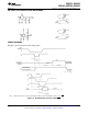
(3) For V
IN
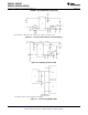
(−)≥ VIN(+) the digital output code will be 0000 0000. Two on-chip diodes are tied to each analog input (see block diagram)
which will forward conduct for analog input voltages one diode drop below ground or one diode drop greater than the V
CC
supply. Be
careful, during testing at low V
CC
levels (4.5V), as high level analog inputs (5V) can cause this input diode to conduct–especially at
elevated temperatures, and cause errors for analog inputs near full-scale. The spec allows 50 mV forward bias of either diode. This
means that as long as the analog V
IN
does not exceed the supply voltage by more than 50 mV, the output code will be correct. To
achieve an absolute 0 V
DC
to 5 V
DC
input voltage range will therefore require a minimum supply voltage of 4.950 V
DC
over temperature
variations, initial tolerance and loading.
Copyright © 2009–2013, Texas Instruments Incorporated Submit Documentation Feedback 3
Product Folder Links: ADC0801, ADC0802 ADC0803, ADC0804, ADC0805