
Datasheet


ADC0801, ADC0802
ADC0803, ADC0804, ADC0805
SNOSBI1B –NOVEMBER 2009–REVISED FEBRUARY 2013
www.ti.com
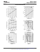
AC ELECTRICAL CHARACTERISTICS
The following specifications apply for V
CC
=5 V
DC
and T
MIN
≤ T
A
≤T
MAX
(unless otherwise specified)
PARAMETER CONDITIONS MIN TYP MAX UNITS
f
CLK
= 640 kHz
(1)
103 114 µs
T
C
Conversion Time
See
(2)(1)
66 73 1/fCLK
Clock Frequency 100 640 1460 kHz
f
CLK
V
CC
= 5V
(2)
Clock Duty Cycle 40% 60%
INTR tied to WR with CS = 0 VDC,
CR Conversion Rate in Free-Running Mode 8770 9708 conv/s
f
CLK
= 640 kHz
t
W(WR)L
Width of WR Input (Start Pulse Width) CS = 0 VDC
(3)
100 ns
Access Time (Delay from Falling Edge of RD
tACC C
L
= 100 pF 135 200 ns
to Output Data Valid)
TRI-STATE Control (Delay from Rising Edge of C
L
= 10 pF, R
L
= 10k (See TRI-STATE
t1H, t0H 125 200 ns
RD to Hi-Z State) TEST CIRCUITS AND WAVEFORMS)
Delay from Falling Edge of WR or RD to Reset
t
WI
, t
RI
300 450 ns
of INTR
C
IN
Input Capacitance of Logic Control Inputs 5 7.5 pF
C
OUT
TRI-STATE Output Capacitance (Data Buffers) 5 7.5 pF
CONTROL INPUTS [Note: CLK IN (Pin 4) is the input of a Schmitt trigger circuit and is therefore specified separately]
V
IN
(1) Logical “1” Input Voltage (Except Pin 4 CLK IN) V
CC
= 5.25 VDC 2 15 V
DC
V
IN
(0) Logical “0” Input Voltage (Except Pin 4 CLK IN) V
CC
= 4.75 VDC 0.8 V
DC
I
IN
(1) Logical “1” Input Current (All Inputs) V
IN
= 5 VDC 0.005 1 µA
DC
I
IN
(0) Logical “0” Input Current (All Inputs) V
IN
= 0 VDC –1 –0.005 µA
DC
CLOCK IN AND CLOCK R
CLK IN (Pin 4) Positive Going Threshold
V
T
+ 2.7 3.1 3.5 V
DC
Voltage
CLK IN (Pin 4) Negative Going Threshold
V
T
− 1.5 1.8 2.1 V
DC
Voltage
V
H
CLK IN (Pin 4) Hysteresis (V
T
+)–(V
T
−) 0.6 1.3 2 V
DC
V
OUT
(0) Logical “0” CLK R Output Voltage I
O
= 360 µA, V
CC
= 4.75 VDC 0.4 V
DC
V
OUT
(1) Logical “1” CLK R Output Voltage I
O
= −360 µA, V
CC
= 4.75 VDC 2.4 V
DC
DATA OUTPUTS AND INTR
Logical “0” Output Voltage
V
OUT
(0) Data Outputs I
OUT
= 1.6 mA, V
CC
= 4.75 V
DC
0.4 V
DC
INTR Output I
OUT
= 1.0 mA, V
CC
= 4.75 V
DC
0.4 V
DC
I
O
= −360 µA, V
CC
= 4.75 V
DC
2.4 V
DC
V
OUT
(1) Logical “1” Output Voltage
I
O
= −10 µA, V
CC
= 4.75 V
DC
4.5 V
DC
V
OUT
= 0 VDC –3 µA
DC
TRI-STATE Disabled Output Leakage (All Data
I
OUT
Buffers)
V
OUT
= 5 VDC 3 µA
DC
I
SOURCE
V
OUT
Short to GND, T
A
= 2 5°C 4.5 6 mA
DC
I
SINK
V
OUT
Short to V
CC
, T
A
= 25°C 9 16 mA
DC
POWER SUPPLY
Supply Current (Includes Ladder Current)
f
CLK
= 640 kHz, V
REF
/2 = NC,
I
CC
ADC0801/02/03/04LCJ/05 1.1 1.8 mA
T
A
= 25°C and CS = 5 V
ADC0804LCN/LCWM 1.9 2.5 mA
(1) Accuracy is specified at f
CLK
= 640 kHz. At higher clock frequencies accuracy can degrade. For lower clock frequencies, the duty cycle
limits can be extended so long as the minimum clock high time interval or minimum clock low time interval is no less than 275 ns.
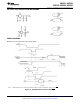
(2) With an asynchronous start pulse, up to 8 clock periods may be required before the internal clock phases are proper to start the
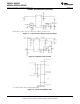
conversion process. The start request is internally latched, see Figure 48 and FUNCTIONAL DESCRIPTION.
(3) The CS input is assumed to bracket the WR strobe input and therefore timing is dependent on the WR pulse width. An arbitrarily wide
pulse width will hold the converter in a reset mode and the start of conversion is initiated by the low to high transition of the WR pulse
(see TIMING DIAGRAMS).
4 Submit Documentation Feedback Copyright © 2009–2013, Texas Instruments Incorporated
Product Folder Links: ADC0801, ADC0802 ADC0803, ADC0804, ADC0805