
Datasheet


ADC0801, ADC0802
ADC0803, ADC0804, ADC0805
www.ti.com
SNOSBI1B –NOVEMBER 2009–REVISED FEBRUARY 2013
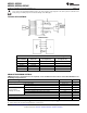
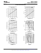
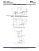
TYPICAL CHARACTERISTICS
spacer
Logic Input Threshold Voltage vs Delay From Falling Edge of RD to Output
Supply Voltage Data Valid vs Load Capacitance
Figure 1. Figure 2.
CLK IN Schmitt Trip Levels vs
Supply Voltage f
CLK
vs Clock Capacitor
Figure 3. Figure 4.
Full-Scale Error vs Effect of Unadjusted Offset Error
Conversion Time V
REF
/2 Voltage
Figure 5. Figure 6.
Copyright © 2009–2013, Texas Instruments Incorporated Submit Documentation Feedback 5
Product Folder Links: ADC0801, ADC0802 ADC0803, ADC0804, ADC0805