ADC0801,ADC0802,ADC0803,ADC0804,ADC0805 ADC0801/ADC0802/ADC0803/ADC0804/ADC0805 8-Bit µP Compatible A/D Converters Literature Number: SNOSBI1A
ADC0801/ADC0802/ADC0803/ADC0804/ADC0805 8-Bit µP Compatible A/D Converters General Description The ADC0801, ADC0802, ADC0803, ADC0804 and ADC0805 are CMOS 8-bit successive approximation A/D converters that use a differential potentiometric ladder — similar to the 256R products. These converters are designed to allow operation with the NSC800 and INS8080A derivative control bus with TRI-STATE output latches directly driving the data bus.
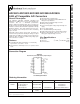
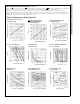
ADC0801/ADC0802/ADC0803/ADC0804/ADC0805 Typical Applications DS005671-1 8080 Interface DS005671-31 Error Specification (Includes Full-Scale, Zero Error, and Non-Linearity) Part Number Full- VREF/2=2.500 VDC VREF/2=No Connection Scale (No Adjustments) (No Adjustments) Adjusted ADC0801 ± 1⁄4 LSB ± 1⁄2 LSB ADC0802 ADC0803 ADC0804 ± ⁄ LSB 12 ± 1 LSB ± 1 LSB ADC0805 www.national.
Infrared (15 seconds) Storage Temperature Range Package Dissipation at TA =25˚C ESD Susceptibility (Note 10) If Military/Aerospace specified devices are required, please contact the National Semiconductor Sales Office/ Distributors for availability and specifications. Supply Voltage (VCC) (Note 3) Voltage Logic Control Inputs At Other Input and Outputs Lead Temp. (Soldering, 10 seconds) Dual-In-Line Package (plastic) Dual-In-Line Package (ceramic) Surface Mount Package Vapor Phase (60 seconds) 6.
ADC0801/ADC0802/ADC0803/ADC0804/ADC0805 AC Electrical Characteristics (Continued) The following specifications apply for VCC =5 VDC and TMIN≤TA≤TMAX unless otherwise specified. Symbol COUT Parameter Conditions Min TRI-STATE Output Typ Max Units 5 7.5 pF Capacitance (Data Buffers) CONTROL INPUTS [Note: CLK IN (Pin 4) is the input of a Schmitt trigger circuit and is therefore specified separately] VIN (1) Logical “1” Input Voltage VCC =5.25 VDC 2.0 15 VDC 0.
(Continued) Note 7: The CS input is assumed to bracket the WR strobe input and therefore timing is dependent on the WR pulse width. An arbitrarily wide pulse width will hold the converter in a reset mode and the start of conversion is initiated by the low to high transition of the WR pulse (see timing diagrams). Note 8: None of these A/Ds requires a zero adjust (see section 2.5.1). To obtain zero code at other analog input voltages see section 2.5 and Figure 7.
ADC0801/ADC0802/ADC0803/ADC0804/ADC0805 TRI-STATE Test Circuits and Waveforms t1H, CL =10 pF t1H DS005671-48 DS005671-47 tr =20 ns t0H t0H, CL =10 pF DS005671-50 DS005671-49 Timing Diagrams tr =20 ns (All timing is measured from the 50% voltage points) DS005671-51 www.national.
ADC0801/ADC0802/ADC0803/ADC0804/ADC0805 Timing Diagrams (All timing is measured from the 50% voltage points) (Continued) Output Enable and Reset with INTR DS005671-52 Note: Read strobe must occur 8 clock periods (8/fCLK) after assertion of interrupt to guarantee reset of INTR . Typical Applications 6800 Interface Ratiometeric with Full-Scale Adjust DS005671-53 DS005671-54 Note: before using caps at VIN or VREF/2, see section 2.3.2 Input Bypass Capacitors. 7 www.national.
ADC0801/ADC0802/ADC0803/ADC0804/ADC0805 Typical Applications (Continued) Absolute with a 2.500V Reference Absolute with a 5V Reference DS005671-56 DS005671-55 *For low power, see also LM385–2.5 Zero-Shift and Span Adjust: 2V ≤ VIN ≤ 5V Span Adjust: 0V ≤ VIN ≤ 3V DS005671-58 DS005671-57 www.national.
(Continued) Directly Converting a Low-Level Signal A µP Interfaced Comparator DS005671-60 DS005671-59 For: VIN(+) > VIN(−) Output=FFHEX For: VIN(+) < VIN(−) Output=00HEX VREF/2=256 mV 1 mV Resolution with µP Controlled Range DS005671-61 VREF/2=128 mV 1 LSB=1 mV VDAC≤VIN≤(VDAC+256 mV) 0 ≤ VDAC < 2.5V 9 www.national.
ADC0801/ADC0802/ADC0803/ADC0804/ADC0805 Typical Applications (Continued) Digitizing a Current Flow DS005671-62 Self-Clocking Multiple A/Ds External Clocking DS005671-64 100 kHz≤fCLK≤1460 kHz DS005671-63 * Use a large R value to reduce loading at CLK R output. www.national.
(Continued) Self-Clocking in Free-Running Mode µP Interface for Free-Running A/D DS005671-65 *After power-up, a momentary grounding of the WR input is needed to guarantee operation. DS005671-66 Operating with “Automotive” Ratiometric Transducers Ratiometric with VREF/2 Forced DS005671-68 DS005671-67 *VIN(−)=0.
ADC0801/ADC0802/ADC0803/ADC0804/ADC0805 Typical Applications (Continued) Handling ± 10V Analog Inputs Low-Cost, µP Interfaced, Temperature-to-Digital Converter DS005671-70 DS005671-71 *Beckman Instruments #694-3-R10K resistor array µP Interfaced Temperature-to-Digital Converter DS005671-72 *Circuit values shown are for 0˚C≤TA≤+128˚C ***Can calibrate each sensor to allow easy replacement, then A/D can be calibrated with a pre-set input voltage. www.national.
(Continued) Handling ± 5V Analog Inputs Read-Only Interface DS005671-34 DS005671-33 *Beckman Instruments #694-3-R10K resistor array µP Interfaced Comparator with Hysteresis Protecting the Input DS005671-9 Diodes are 1N914 DS005671-35 13 www.national.
ADC0801/ADC0802/ADC0803/ADC0804/ADC0805 Typical Applications (Continued) Analog Self-Test for a System DS005671-36 A Low-Cost, 3-Decade Logarithmic Converter DS005671-37 *LM389 transistors A, B, C, D = LM324A quad op amp www.national.
ADC0801/ADC0802/ADC0803/ADC0804/ADC0805 Typical Applications (Continued) 3-Decade Logarithmic A/D Converter DS005671-73 Noise Filtering the Analog Input Multiplexing Differential Inputs DS005671-74 DS005671-75 fC =20 Hz Uses Chebyshev implementation for steeper roll-off unity-gain, 2nd order, low-pass filter Adding a separate filter for each channel increases system response time if an analog multiplexer is used Output Buffers with A/D Data Enabled Increasing Bus Drive and/or Reducing Time on Bus
ADC0801/ADC0802/ADC0803/ADC0804/ADC0805 Typical Applications (Continued) Sampling an AC Input Signal DS005671-78 Note 11: Oversample whenever possible [keep fs > 2f(−60)] to eliminate input frequency folding (aliasing) and to allow for the skirt response of the filter. Note 12: Consider the amplitude errors which are introduced within the passband of the filter. 70% Power Savings by Clock Gating DS005671-79 (Complete shutdown takes ≈ 30 seconds.
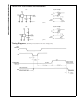
Next to each transfer function is shown the corresponding error plot. Many people may be more familiar with error plots than transfer functions. The analog input voltage to the A/D is provided by either a linear ramp or by the discrete output steps of a high resolution DAC. Notice that the error is continuously displayed and includes the quantization uncertainty of the A/D.
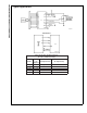
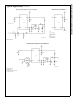
ADC0801/ADC0802/ADC0803/ADC0804/ADC0805 Functional Description (Continued) Error Plot Transfer Function DS005671-85 DS005671-86 FIGURE 3. Clarifying the Error Specs of an A/D Converter Accuracy= ± 1⁄2 LSB A functional diagram of the A/D converter is shown in Figure 4. All of the package pinouts are shown and the major logic control paths are drawn in heavier weight lines. The converter is started by having CS and WR simultaneously low.
ADC0801/ADC0802/ADC0803/ADC0804/ADC0805 Functional Description (Continued) DS005671-13 Note 13: CS shown twice for clarity. Note 14: SAR = Successive Approximation Register. FIGURE 4. Block Diagram After the “1” is clocked through the 8-bit shift register (which completes the SAR search) it appears as the input to the D-type latch, LATCH 1. As soon as this “1” is output from the shift register, the AND gate, G2, causes the new digital word to transfer to the TRI-STATE output latches.
ADC0801/ADC0802/ADC0803/ADC0804/ADC0805 Functional Description (Continued) 2.2 Analog Differential Voltage Inputs and Common-Mode Rejection This A/D has additional applications flexibility due to the analog differential voltage input. The VIN(−) input (pin 7) can be used to automatically subtract a fixed voltage value from the input reading (tare correction). This is also useful in 4 mA–20 mA current loop conversion. In addition, common-mode noise can be reduced by use of the differential input.
Notice that the reference voltage for the IC is either 1⁄2 of the voltage applied to the VCC supply pin, or is equal to the voltage that is externally forced at the VREF/2 pin. This allows for a ratiometric voltage reference using the VCC supply, a 5 VDC reference voltage can be used for the VCC supply or a voltage less than 2.5 VDC can be applied to the VREF/2 input for increased application flexibility.
ADC0801/ADC0802/ADC0803/ADC0804/ADC0805 Functional Description (Continued) DS005671-87 a) Analog Input Signal Example DS005671-88 *Add if VREF/2 ≤ 1 VDC with LM358 to draw 3 mA to ground. b) Accommodating an Analog Input from 0.5V (Digital Out = 00HEX) to 3.5V (Digital Out=FFHEX) FIGURE 7. Adapting the A/D Analog Input Voltages to Match an Arbitrary Input Signal Range 2.
(low power Schottky such as the DM74LS240 series is recommended) or special higher drive current products which are designed as bus drivers. High current bipolar bus drivers with PNP inputs are recommended. (Continued) 2.10 Power Supplies Noise spikes on the VCC supply line can cause conversion errors as the comparator will respond to this noise. A low inductance tantalum filter capacitor should be used close to the converter VCC pin and values of 1 µF or greater are recommended.
ADC0801/ADC0802/ADC0803/ADC0804/ADC0805 Functional Description For a higher speed test system, or to obtain plotted data, a digital-to-analog converter is needed for the test set-up. An accurate 10-bit DAC can serve as the precision voltage source for the A/D. Errors of the A/D under test can be expressed as either analog voltages or differences in 2 digital words. (Continued) A basic A/D tester that uses a DAC and provides the error as an analog output voltage is shown in Figure 8.
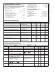
ADC0801/ADC0802/ADC0803/ADC0804/ADC0805 Functional Description (Continued) DS005671-89 FIGURE 10. A/D Tester with Analog Error Output DS005671-90 FIGURE 11. Basic “Digital” A/D Tester TABLE 1. DECODING THE DIGITAL OUTPUT LEDs OUTPUT VOLTAGE FRACTIONAL BINARY VALUE FOR HEX CENTER VALUES BINARY WITH VREF/2=2.
ADC0801/ADC0802/ADC0803/ADC0804/ADC0805 Functional Description (Continued) DS005671-20 Note 16: *Pin numbers for the DP8228 system controller, others are INS8080A. Note 17: Pin 23 of the INS8228 must be tied to +12V through a 1 kΩ resistor to generate the RST 7 instruction when an interrupt is acknowledged as required by the accompanying sample program. FIGURE 12. ADC0801_INS8080A CPU Interface www.national.
ADC0801/ADC0802/ADC0803/ADC0804/ADC0805 Functional Description (Continued) SAMPLE PROGRAM FOR Figure 12 ADC0801–INS8080A CPU INTERFACE DS005671-99 Note 18: The stack pointer must be dimensioned because a RST 7 instruction pushes the PC onto the stack. Note 19: All address used were arbitrarily chosen.
ADC0801/ADC0802/ADC0803/ADC0804/ADC0805 Functional Description (Continued) DS005671-21 FIGURE 13. INS8048 Interface SAMPLE PROGRAM FOR Figure 13 INS8048 INTERFACE DS005671-A0 4.2 Interfacing the Z-80 The Z-80 control bus is slightly different from that of the 8080. General RD and WR strobes are provided and separate memory request, MREQ, and I/O request, IORQ, signals are used which have to be combined with the generalized strobes to provide the equivalent 8080 signals.
already memory mapped in the M6800 system and no CS decoding is necessary. Also notice that the A/D output data lines are connected to the microprocessor bus under program control through the PIA and therefore the A/D RD pin can be grounded. (Continued) A15) during I/O input instructions. For example, MUX channel selection for the A/D can be accomplished with this operating mode. A sample interface program equivalent to the previous one is shown below Figure 16.
ADC0801/ADC0802/ADC0803/ADC0804/ADC0805 Functional Description (Continued) SAMPLE PROGRAM FOR Figure 15 ADC0801-MC6800 CPU INTERFACE DS005671-A1 Note 22: In order for the microprocessor to service subroutines and interrupts, the stack pointer must be dimensioned in the user’s program. DS005671-25 FIGURE 16. ADC0801–MC6820 PIA Interface www.national.
ADC0801/ADC0802/ADC0803/ADC0804/ADC0805 Functional Description (Continued) SAMPLE PROGRAM FOR Figure 16 ADC0801–MC6820 PIA INTERFACE DS005671-A2 The following schematic and sample subroutine (DATA IN) may be used to interface (up to) 8 ADC0801’s directly to the MC6800 CPU. This scheme can easily be extended to allow the interface of more converters. In this configuration the converters are (arbitrarily) located at HEX address 5000 in the MC6800 memory space.
ADC0801/ADC0802/ADC0803/ADC0804/ADC0805 Functional Description (Continued) DS005671-26 Note 23: Numbers in parentheses refer to MC6800 CPU pin out. Note 24: Numbers of letters in brackets refer to standard M6800 system common bus code. FIGURE 17. Interfacing Multiple A/Ds in an MC6800 System www.national.
ADC0801/ADC0802/ADC0803/ADC0804/ADC0805 Functional Description (Continued) SAMPLE PROGRAM FOR Figure 17 INTERFACING MULTIPLE A/D’s IN AN MC6800 SYSTEM DS005671-A3 SAMPLE PROGRAM FOR Figure 17 INTERFACING MULTIPLE A/D’s IN AN MC6800 SYSTEM DS005671-A4 Note 25: In order for the microprocessor to service subroutines and interrupts, the stack pointer must be dimensioned in the user’s program.
ADC0801/ADC0802/ADC0803/ADC0804/ADC0805 Functional Description the ADC0801. It is important that the voltage levels that drive the auto-zero resistors be constant. Also, for symmetry, a logic swing of 0V to 5V is convenient. To achieve this, a CMOS buffer is used for the logic output signals of Port B and this CMOS package is powered with a stable 5V source. Buffer amplifier A1 is necessary so that it can source or sink the D/A output current.
ADC0801/ADC0802/ADC0803/ADC0804/ADC0805 Functional Description (Continued) DS005671-92 FIGURE 19. Microprocessor Interface Circuitry for Differential Preamp A flow chart for the zeroing subroutine is shown in Figure 20. It must be noted that the ADC0801 series will output an all zero code when it converts a negative input [VIN(−) ≥ VIN(+)]. Also, a logic inversion exists as all of the I/O ports are buffered with inverting gates.
ADC0801/ADC0802/ADC0803/ADC0804/ADC0805 Functional Description (Continued) DS005671-28 FIGURE 20. Flow Chart for Auto-Zero Routine www.national.
ADC0801/ADC0802/ADC0803/ADC0804/ADC0805 Functional Description (Continued) DS005671-A5 Note 29: All numerical values are hexadecimal representations. FIGURE 21. Software for Auto-Zeroed Differential A/D 5.3 Multiple A/D Converters in a Z-80 Interrupt Driven Mode (Continued) The following notes apply: • It is assumed that the CPU automatically performs a RST 7 instruction when a valid interrupt is acknowledged (CPU is in interrupt mode 1). Hence, the subroutine starting address of X0038.
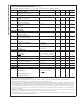
ADC0801/ADC0802/ADC0803/ADC0804/ADC0805 Functional Description (Continued) HEX PORT ADDRESS PERIPHERAL 04 A/D 4 HEX PORT ADDRESS PERIPHERAL 05 A/D 5 00 MM74C374 8-bit flip-flop 06 A/D 6 01 A/D 1 02 A/D 2 03 A/D 3 07 A/D 7 This port address also serves as the A/D identifying word in the program. DS005671-29 FIGURE 22. Multiple A/Ds with Z-80 Type Microprocessor www.national.
ADC0801/ADC0802/ADC0803/ADC0804/ADC0805 Functional Description (Continued) DS005671-A6 39 www.national.
ADC0801/ADC0802/ADC0803/ADC0804/ADC0805 Physical Dimensions inches (millimeters) unless otherwise noted SO Package (M) Order Number ADC0802LCWM or ADC0804LCWM NS Package Number M20B Molded Dual-In-Line Package (N) Order Number ADC0801LCN, ADC0802LCN, ADC0803LCN, ADC0804LCN or ADC0805LCN NS Package Number N20A www.national.
LIFE SUPPORT POLICY NATIONAL’S PRODUCTS ARE NOT AUTHORIZED FOR USE AS CRITICAL COMPONENTS IN LIFE SUPPORT DEVICES OR SYSTEMS WITHOUT THE EXPRESS WRITTEN APPROVAL OF THE PRESIDENT AND GENERAL COUNSEL OF NATIONAL SEMICONDUCTOR CORPORATION. As used herein: 1.
IMPORTANT NOTICE Texas Instruments Incorporated and its subsidiaries (TI) reserve the right to make corrections, modifications, enhancements, improvements, and other changes to its products and services at any time and to discontinue any product or service without notice. Customers should obtain the latest relevant information before placing orders and should verify that such information is current and complete.