
Datasheet

Functional Description (Continued)
±
1
⁄
2
LSB from the ideal center-values. Each tread (the range
of analog input voltage that provides the same digital output
code) is therefore 1 LSB wide.
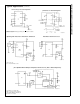
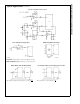
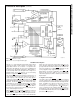
Figure 2
shows a worst case error plot for the ADC0801. All
center-valued inputs are guaranteed to produce the correct
output codes and the adjacent risers are guaranteed to be
no closer to the center-value points than
±
1
⁄
4
LSB. In other
words, if we apply an analog input equal to the center-value
±
1
⁄
4
LSB,
we guarantee
that the A/D will produce the correct
digital code. The maximum range of the position of the code
transition is indicated by the horizontal arrow and it is guar-
anteed to be no more than
1
⁄
2
LSB.
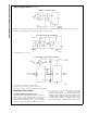
The error curve of
Figure 3
shows a worst case error plot for
the ADC0802. Here we guarantee that if we apply an analog
input equal to the LSB analog voltage center-value the A/D
will produce the correct digital code.
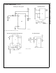
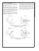
Next to each transfer function is shown the corresponding
error plot. Many people may be more familiar with error plots
than transfer functions. The analog input voltage to the A/D
is provided by either a linear ramp or by the discrete output
steps of a high resolution DAC. Notice that the error is
continuously displayed and includes the quantization uncer-
tainty of the A/D. For example the error at point 1 of
Figure 1
is +
1
⁄
2
LSB because the digital code appeared
1
⁄
2
LSB in
advance of the center-value of the tread. The error plots
always have a constant negative slope and the abrupt up-
side steps are always 1 LSB in magnitude.
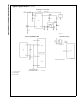
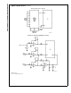
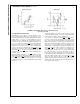
Transfer Function
DS005671-81
Error Plot
DS005671-82
FIGURE 1. Clarifying the Error Specs of an A/D Converter
Accuracy=
±
0 LSB: A Perfect A/D
Transfer Function
DS005671-83
Error Plot
DS005671-84
FIGURE 2. Clarifying the Error Specs of an A/D Converter
Accuracy=
±
1
⁄
4
LSB
ADC0801/ADC0802/ADC0803/ADC0804/ADC0805
www.national.com17