
Datasheet

Functional Description (Continued)
2.2 Analog Differential Voltage Inputs and
Common-Mode Rejection
This A/D has additional applications flexibility due to the
analog differential voltage input. The V
IN
(−) input (pin 7) can
be used to automatically subtract a fixed voltage value from
the input reading (tare correction). This is also useful in 4
mA–20 mA current loop conversion. In addition,
common-mode noise can be reduced by use of the differen-
tial input.
The time interval between sampling V
IN
(+) and V
IN
(−) is 4-
1
⁄
2
clock periods. The maximum error voltage due to this slight
time difference between the input voltage samples is given
by:
where:
∆V
e
is the error voltage due to sampling delay
V
P
is the peak value of the common-mode voltage
f
cm
is the common-mode frequency
As an example, to keep this error to
1
⁄
4
LSB (∼5 mV) when
operating with a 60 Hz common-mode frequency, f
cm
, and
using a 640 kHz A/D clock, f
CLK
, would allow a peak value of
the common-mode voltage, V
P
, which is given by:
or
which gives
V
P
.1.9V.
The allowed range of analog input voltages usually places
more severe restrictions on input common-mode noise lev-
els.
An analog input voltage with a reduced span and a relatively
large zero offset can be handled easily by making use of the
differential input (see section 2.4 Reference Voltage).
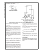
2.3 Analog Inputs
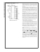
2.3 1 Input Current
Normal Mode
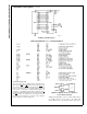
Due to the internal switching action, displacement currents
will flow at the analog inputs. This is due to on-chip stray
capacitance to ground as shown in
Figure 5
.
The voltage on this capacitance is switched and will result in
currents entering the V
IN
(+) input pin and leaving the V
IN
(−)
input which will depend on the analog differential input volt-
age levels. These current transients occur at the leading
edge of the internal clocks. They rapidly decay and
do not
cause errors
as the on-chip comparator is strobed at the end
of the clock period.
Fault Mode
If the voltage source applied to the V
IN
(+) or V
IN
(−) pin
exceeds the allowed operating range of V
CC
+50 mV, large
input currents can flow through a parasitic diode to the V
CC
pin. If these currents can exceed the 1 mA max allowed
spec, an external diode (1N914) should be added to bypass
this current to the V
CC
pin (with the current bypassed with
this diode, the voltage at the V
IN
(+) pin can exceed the V
CC
voltage by the forward voltage of this diode).
2.3.2 Input Bypass Capacitors
Bypass capacitors at the inputs will average these charges
and cause a DC current to flow through the output resis-
tances of the analog signal sources. This charge pumping
action is worse for continuous conversions with the V
IN
(+)
input voltage at full-scale. For continuous conversions with a
640 kHz clock frequency with the V
IN
(+) input at 5V, this DC
current is at a maximum of approximately 5 µA. Therefore,
bypass capacitors should not be used at the analog inputs or
the V
REF
/2 pin
for high resistance sources (
>
1kΩ). If input
bypass capacitors are necessary for noise filtering and high
source resistance is desirable to minimize capacitor size, the
detrimental effects of the voltage drop across this input
resistance, which is due to the average value of the input
current, can be eliminated with a full-scale adjustment while
the given source resistor and input bypass capacitor are
both in place. This is possible because the average value of
the input current is a precise linear function of the differential
input voltage.
2.3.3 Input Source Resistance
Large values of source resistance where an input bypass
capacitor is not used,
will not cause errors
as the input
currents settle out prior to the comparison time. If a low pass
filter is required in the system, use a low valued series
resistor (≤ 1kΩ) for a passive RC section or add an op amp
RC active low pass filter. For low source resistance applica-
tions, (≤ 1kΩ), a 0.1 µF bypass capacitor at the inputs will
prevent noise pickup due to series lead inductance of a long
DS005671-14
r
ON
of SW 1 and SW 2 . 5kΩ
r=r
ON
C
STRAY
. 5kΩx12pF=60ns
FIGURE 5. Analog Input Impedance
ADC0801/ADC0802/ADC0803/ADC0804/ADC0805
www.national.com 20