
Datasheet

Functional Description (Continued)
wire. A 100Ω series resistor can be used to isolate this
capacitor—both the R and C are placed outside the feed-
back loop — from the output of an op amp, if used.
2.3.4 Noise
The leads to the analog inputs (pins 6 and 7) should be kept
as short as possible to minimize input noise coupling. Both
noise and undesired digital clock coupling to these inputs
can cause system errors. The source resistance for these
inputs should, in general, be kept below 5 kΩ. Larger values
of source resistance can cause undesired system noise
pickup. Input bypass capacitors, placed from the analog
inputs to ground, will eliminate system noise pickup but can
create analog scale errors as these capacitors will average
the transient input switching currents of the A/D (see section
2.3.1.). This scale error depends on both a large source
resistance and the use of an input bypass capacitor. This
error can be eliminated by doing a full-scale adjustment of
the A/D (adjust V
REF
/2 for a proper full-scale reading — see
section 2.5.2 on Full-Scale Adjustment) with the source re-
sistance and input bypass capacitor in place.
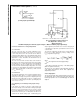
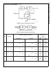
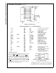
2.4 Reference Voltage
2.4.1 Span Adjust
For maximum applications flexibility, these A/Ds have been
designed to accommodatea5V
DC
, 2.5 V
DC
or an adjusted
voltage reference. This has been achieved in the design of
the IC as shown in
Figure 6
.
Notice that the reference voltage for the IC is either
1
⁄
2
of the
voltage applied to the V
CC
supply pin, or is equal to the
voltage that is externally forced at the V
REF
/2 pin. This allows
for a ratiometric voltage reference using the V
CC
supply, a 5
V
DC
reference voltage can be used for the V
CC
supply or a
voltage less than 2.5 V
DC
can be applied to the V
REF
/2 input
for increased application flexibility. The internal gain to the
V
REF
/2 input is 2, making the full-scale differential input
voltage twice the voltage at pin 9.
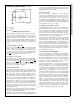
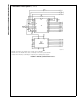
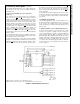
An example of the use of an adjusted reference voltage is to
accommodate a reduced span—or dynamic voltage range
of the analog input voltage. If the analog input voltage were
to range from 0.5 V
DC
to 3.5 V
DC
, instead of 0V to 5 V
DC
, the
span would be 3V as shown in
Figure 7
. With 0.5 V
DC
applied to the V
IN
(−) pin to absorb the offset, the reference
voltage can be made equal to
1
⁄
2
of the 3V span or 1.5 V
DC
.
The A/D now will encode the V
IN
(+) signal from 0.5V to 3.5 V
with the 0.5V input corresponding to zero and the 3.5 V
DC
input corresponding to full-scale. The full 8 bits of resolution
are therefore applied over this reduced analog input voltage
range.
2.4.2 Reference Accuracy Requirements
The converter can be operated in a ratiometric mode or an
absolute mode. In ratiometric converter applications, the
magnitude of the reference voltage is a factor in both the
output of the source transducer and the output of the A/D
converter and therefore cancels out in the final digital output
code. The ADC0805 is specified particularly for use in ratio-
metric applications with no adjustments required. In absolute
conversion applications, both the initial value and the tem-
perature stability of the reference voltage are important fac-
tors in the accuracy of the A/D converter. For V
REF
/2 volt-
ages of 2.4 V
DC
nominal value, initial errors of
±
10 mV
DC
will
cause conversion errors of
±
1 LSB due to the gain of 2 of the
V
REF
/2 input. In reduced span applications, the initial value
and the stability of the V
REF
/2 input voltage become even
more important. For example, if the span is reduced to 2.5V,
the analog input LSB voltage value is correspondingly re-
duced from 20 mV (5V span) to 10 mV and 1 LSB at the
V
REF
/2 input becomes 5 mV. As can be seen, this reduces
the allowed initial tolerance of the reference voltage and
requires correspondingly less absolute change with tem-
perature variations. Note that spans smaller than 2.5V place
even tighter requirements on the initial accuracy and stability
of the reference source.
In general, the magnitude of the reference voltage will re-
quire an initial adjustment. Errors due to an improper value
of reference voltage appear as full-scale errors in the A/D
transfer function. IC voltage regulators may be used for
references if the ambient temperature changes are not ex-
cessive. The LM336B 2.5V IC reference diode (from Na-
tional Semiconductor) has a temperature stability of 1.8 mV
typ (6 mV max) over 0˚C≤T
A
≤+70˚C. Other temperature
range parts are also available.
DS005671-15
FIGURE 6. The V
REFERENCE
Design on the IC
ADC0801/ADC0802/ADC0803/ADC0804/ADC0805
www.national.com21