
Datasheet

Functional Description (Continued)
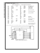
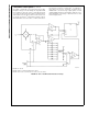
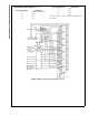
any output of Port B will source current into node V
X
thus
raising the voltage at V
X
and making the output differential
more negative. Conversely, a logic “0” (0V) will pull current
out of node V
X
and decrease the voltage, causing the differ-
ential output to become more positive. For the resistor val-
ues shown, V
X
can move
±
12 mV with a resolution of 50 µV,
which will null the offset error term to
1
⁄
4
LSB of full-scale for
the ADC0801. It is important that the voltage levels that drive
the auto-zero resistors be constant. Also, for symmetry, a
logic swing of 0V to 5V is convenient. To achieve this, a
CMOS buffer is used for the logic output signals of Port B
and this CMOS package is powered with a stable 5V source.
Buffer amplifier A1 is necessary so that it can source or sink
the D/A output current.
DS005671-91
Note 26: R2 = 49.5 R1
Note 27: Switches are LMC13334 CMOS analog switches.
Note 28: The 9 resistors used in the auto-zero section can be
±
5% tolerance.
FIGURE 18. Gain of 100 Differential Transducer Preamp
ADC0801/ADC0802/ADC0803/ADC0804/ADC0805
www.national.com 34