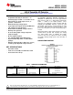
ADC0801, ADC0802 ADC0803, ADC0804, ADC0805 www.ti.com SNOSBI1B – NOVEMBER 2009 – REVISED FEBRUARY 2013 8-Bit µP Compatible A/D Converters Check for Samples: ADC0801, ADC0802, ADC0803, ADC0804, ADC0805 FEATURES DESCRIPTION • The ADC0801, ADC0802, ADC0803, ADC0804 and ADC0805 are CMOS 8-bit successive approximation A/D converters that use a differential potentiometric ladder — similar to the 256R products.
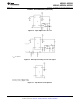
ADC0801, ADC0802 ADC0803, ADC0804, ADC0805 SNOSBI1B – NOVEMBER 2009 – REVISED FEBRUARY 2013 www.ti.com These devices have limited built-in ESD protection. The leads should be shorted together or the device placed in conductive foam during storage or handling to prevent electrostatic damage to the MOS gates. TYPICAL APPLICATIONS 8080 Interface ERROR SPECIFICATION (Includes Full-Scale, Zero Error, and Non-Linearity) PART NUMBER FULL-SCALE ADJUSTED ADC0801 ±1⁄4 LSB ADC0802 VREF/2 = 2.
ADC0801, ADC0802 ADC0803, ADC0804, ADC0805 www.ti.com SNOSBI1B – NOVEMBER 2009 – REVISED FEBRUARY 2013 OPERATING RATINGS (1) (2) over operating free-air temperature range (unless otherwise noted) TMIN ≤ TA ≤ TMAX Temperature Range ADC0804LCJ –40°C ≤ TA ≤ +85°C ADC0801/02/03/05LCN –40°C ≤ TA ≤ +85°C ADC0804LCN 0°C ≤ TA ≤ +70°C ADC0802/04LCWM 0°C ≤ TA ≤ +70°C Range of VCC (1) (2) 4.5 VDC to 6.3 VDC Absolute Maximum Ratings indicate limits beyond which damage to the device may occur.
ADC0801, ADC0802 ADC0803, ADC0804, ADC0805 SNOSBI1B – NOVEMBER 2009 – REVISED FEBRUARY 2013 www.ti.
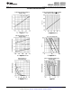
ADC0801, ADC0802 ADC0803, ADC0804, ADC0805 www.ti.com SNOSBI1B – NOVEMBER 2009 – REVISED FEBRUARY 2013 TYPICAL CHARACTERISTICS spacer Logic Input Threshold Voltage vs Supply Voltage Delay From Falling Edge of RD to Output Data Valid vs Load Capacitance Figure 1. Figure 2. CLK IN Schmitt Trip Levels vs Supply Voltage fCLK vs Clock Capacitor Figure 3. Figure 4. Full-Scale Error vs Conversion Time Effect of Unadjusted Offset Error VREF/2 Voltage Figure 5. Figure 6.
ADC0801, ADC0802 ADC0803, ADC0804, ADC0805 SNOSBI1B – NOVEMBER 2009 – REVISED FEBRUARY 2013 www.ti.com TYPICAL CHARACTERISTICS (continued) spacer Output Current Temperature Power Supply Current vs Temperature (1) Figure 7. Figure 8. Linearity Error at Low VREF/2 Voltages Figure 9. (1) 6 The VREF/2 pin is the center point of a two-resistor divider connected from VCC to ground. In all versions of the ADC0801, ADC0802, ADC0803, and ADC0805, and in the ADC0804LCJ, each resistor is typically 16 kΩ.
ADC0801, ADC0802 ADC0803, ADC0804, ADC0805 www.ti.com SNOSBI1B – NOVEMBER 2009 – REVISED FEBRUARY 2013 TRI-STATE TEST CIRCUITS AND WAVEFORMS SPACER SPACER TIMING DIAGRAMS All timing is measured from the 50% voltage points Note: Read strobe must occur 8 clock periods (8/fCLK) after assertion of interrupt to specify reset of INTR. Figure 10.
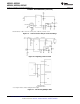
ADC0801, ADC0802 ADC0803, ADC0804, ADC0805 SNOSBI1B – NOVEMBER 2009 – REVISED FEBRUARY 2013 www.ti.com TYPICAL APPLICATIONS Figure 11. 6800 Interface Note: before using caps at VIN or VREF/2, see section Input Bypass Capacitors. Figure 13. Ratiometeric with Full-Scale Adjust *For low power, see also LM385–2.5 Figure 12. Absolute with a 2.500V Reference Figure 14. Absolute with a 5V Reference Figure 15.
ADC0801, ADC0802 ADC0803, ADC0804, ADC0805 www.ti.com SNOSBI1B – NOVEMBER 2009 – REVISED FEBRUARY 2013 TYPICAL APPLICATIONS (continued) Figure 16. Span Adjust: 0V ≤ VIN ≤ 3V VREF/2 = 256 mV Figure 17. Directly Converting a Low-Level Signal For: VIN(+)>VIN(−); Output = FFHEX For: VIN(+) < VIN(−); Output = 00HEX Figure 18.
ADC0801, ADC0802 ADC0803, ADC0804, ADC0805 SNOSBI1B – NOVEMBER 2009 – REVISED FEBRUARY 2013 www.ti.com TYPICAL APPLICATIONS (continued) VREF/2=128 mV; 1 LSB =1 mV; VDAC ≤ VIN ≤ (VDAC + 256 mV); 0 ≤ VDAC < 2.5 V Figure 19. 1 mV Resolution with µP Controlled Range Figure 20. Digitizing a Current Flow * Use a large R value to reduce loading at CLK R output. Figure 21.
ADC0801, ADC0802 ADC0803, ADC0804, ADC0805 www.ti.com SNOSBI1B – NOVEMBER 2009 – REVISED FEBRUARY 2013 TYPICAL APPLICATIONS (continued) *After power-up, a momentary grounding of the WR input is needed to ensure operation. Figure 22. Self-Clocking in Free-Running Mode Figure 23. µP Interface for Free-Running A/D J 100 kHz ≤ fCLK ≤ 1460 kHz Figure 24. External clocking *VIN(−) = 0.15 VCC 15% of VCC ≤ VXDR ≤ 85% of VCC Figure 25. Operating with “Automotive” Ratiometric Transducers Figure 26.
ADC0801, ADC0802 ADC0803, ADC0804, ADC0805 SNOSBI1B – NOVEMBER 2009 – REVISED FEBRUARY 2013 www.ti.com TYPICAL APPLICATIONS (continued) *See Figure 48 to select R value DB7 = “1” for VIN(+)>VIN(−)+(VREF/2). Omit circuitry within the dotted area if hysteresis is not needed. Figure 27. µP Compatible Differential-Input Comparator with Pre-Set VOS (with or without Hysteresis) *Beckman Instruments #694-3-R10K resistor array Figure 28. Handling ±10V Analog Inputs Figure 29.
ADC0801, ADC0802 ADC0803, ADC0804, ADC0805 www.ti.com SNOSBI1B – NOVEMBER 2009 – REVISED FEBRUARY 2013 TYPICAL APPLICATIONS (continued) *Beckman Instruments #694-3-R10K resistor array Figure 31. Handling ±5V Analog Inputs Figure 32. Read-Only Interface Copyright © 2009–2013, Texas Instruments Incorporated Figure 33.
ADC0801, ADC0802 ADC0803, ADC0804, ADC0805 SNOSBI1B – NOVEMBER 2009 – REVISED FEBRUARY 2013 www.ti.com TYPICAL APPLICATIONS (continued) Diodes are 1N914 Figure 34. Protecting the Input Figure 35. Analog Self-Test for a System *LM389 transistors A, B, C, D = LM324A quad op amp Figure 36.
ADC0801, ADC0802 ADC0803, ADC0804, ADC0805 www.ti.com SNOSBI1B – NOVEMBER 2009 – REVISED FEBRUARY 2013 TYPICAL APPLICATIONS (continued) fC=20 Hz Uses Chebyshev implementation for steeper roll-off unity-gain, 2nd order, low-pass filter Adding a separate filter for each channel increases system response time if an analog multiplexer is used Figure 37. 3-Decade Logarithmic A/D Converter Figure 38. Noise Filtering the Analog Input Figure 40.
ADC0801, ADC0802 ADC0803, ADC0804, ADC0805 SNOSBI1B – NOVEMBER 2009 – REVISED FEBRUARY 2013 www.ti.com TYPICAL APPLICATIONS (continued) (1) Oversample whenever possible [keep fs > 2f(−60)] to eliminate input frequency folding (aliasing) and to allow for the skirt response of the filter. (2) Consider the amplitude errors which are introduced within the passband of the filter. Figure 42. Sampling an AC Input Signal (Complete shutdown takes ≈ 30 seconds.) Figure 43.
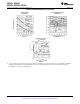
ADC0801, ADC0802 ADC0803, ADC0804, ADC0805 www.ti.com SNOSBI1B – NOVEMBER 2009 – REVISED FEBRUARY 2013 FUNCTIONAL DESCRIPTION Understanding A/D Error Specs A perfect A/D transfer characteristic (staircase waveform) is shown in Figure 45. The horizontal scale is analog input voltage and the particular points labeled are in steps of 1 LSB (19.53 mV with 2.5V tied to the VREF/2 pin). The digital output codes that correspond to these inputs are shown as D−1, D, and D+1.
ADC0801, ADC0802 ADC0803, ADC0804, ADC0805 SNOSBI1B – NOVEMBER 2009 – REVISED FEBRUARY 2013 www.ti.com Figure 47. Clarifying the Error Specs of an A/D Converter Accuracy = ±1⁄2 LSB Functional Description The ADC0801 series contains a circuit equivalent of the 256R network. Analog switches are sequenced by successive approximation logic to match the analog difference input voltage [VIN(+) − VIN(−)] to a corresponding tap on the R network.
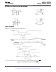
ADC0801, ADC0802 ADC0803, ADC0804, ADC0805 www.ti.com SNOSBI1B – NOVEMBER 2009 – REVISED FEBRUARY 2013 (1) CS shown twice for clarity. (2) SAR = Successive Approximation Register. Figure 48. Block Diagram After the “1” is clocked through the 8-bit shift register (which completes the SAR search) it appears as the input to the D-type latch, LATCH 1. As soon as this “1” is output from the shift register, the AND gate, G2, causes the new digital word to transfer to the TRI-STATE output latches.
ADC0801, ADC0802 ADC0803, ADC0804, ADC0805 SNOSBI1B – NOVEMBER 2009 – REVISED FEBRUARY 2013 www.ti.com Digital Control Inputs The digital control inputs (CS, RD, and WR) meet standard T2L logic voltage levels. These signals have been renamed when compared to the standard A/D Start and Output Enable labels. In addition, these inputs are active low to allow an easy interface to microprocessor control busses.
ADC0801, ADC0802 ADC0803, ADC0804, ADC0805 www.ti.com SNOSBI1B – NOVEMBER 2009 – REVISED FEBRUARY 2013 rON of SW 1 and SW 2 . 5 kΩ r=rON CSTRAY × 5 kΩ x 12 pF = 60 ns Figure 49. Analog Input Impedance The voltage on this capacitance is switched and will result in currents entering the VIN(+) input pin and leaving the VIN(−) input which will depend on the analog differential input voltage levels. These current transients occur at the leading edge of the internal clocks.
ADC0801, ADC0802 ADC0803, ADC0804, ADC0805 SNOSBI1B – NOVEMBER 2009 – REVISED FEBRUARY 2013 www.ti.com Noise The leads to the analog inputs (pins 6 and 7) should be kept as short as possible to minimize input noise coupling. Both noise and undesired digital clock coupling to these inputs can cause system errors. The source resistance for these inputs should, in general, be kept below 5 kΩ. Larger values of source resistance can cause undesired system noise pickup.
ADC0801, ADC0802 ADC0803, ADC0804, ADC0805 www.ti.com SNOSBI1B – NOVEMBER 2009 – REVISED FEBRUARY 2013 Reference Voltage Span Adjust For maximum applications flexibility, these A/Ds have been designed to accommodate a 5 VDC, 2.5 VDC or an adjusted voltage reference. This has been achieved in the design of the IC as shown in Figure 50. Figure 50.
ADC0801, ADC0802 ADC0803, ADC0804, ADC0805 SNOSBI1B – NOVEMBER 2009 – REVISED FEBRUARY 2013 www.ti.com In general, the magnitude of the reference voltage will require an initial adjustment. Errors due to an improper value of reference voltage appear as full-scale errors in the A/D transfer function. IC voltage regulators may be used for references if the ambient temperature changes are not excessive. The LM336B 2.5V IC reference diode (from National Semiconductor) has a temperature stability of 1.
ADC0801, ADC0802 ADC0803, ADC0804, ADC0805 www.ti.com SNOSBI1B – NOVEMBER 2009 – REVISED FEBRUARY 2013 (4) where: VMAX = The high end of the analog input range and VMIN = the low end (the offset zero) of the analog range. (Both are ground referenced.) The VREF/2 (or VCC) voltage is then adjusted to provide a code change from FEHEX to FFHEX.
ADC0801, ADC0802 ADC0803, ADC0804, ADC0805 SNOSBI1B – NOVEMBER 2009 – REVISED FEBRUARY 2013 www.ti.com There are some alternatives available to the designer to handle this problem. Basically, the capacitive loading of the data bus slows down the response time, even though DC specifications are still met.
ADC0801, ADC0802 ADC0803, ADC0804, ADC0805 www.ti.com SNOSBI1B – NOVEMBER 2009 – REVISED FEBRUARY 2013 Figure 53. Basic A/D Tester For a higher speed test system, or to obtain plotted data, a digital-to-analog converter is needed for the test setup. An accurate 10-bit DAC can serve as the precision voltage source for the A/D. Errors of the A/D under test can be expressed as either analog voltages or differences in 2 digital words.
ADC0801, ADC0802 ADC0803, ADC0804, ADC0805 SNOSBI1B – NOVEMBER 2009 – REVISED FEBRUARY 2013 www.ti.com Figure 54. A/D Tester with Analog Error Output Figure 55. Basic “Digital” A/D Tester Table 2. Decoding the Digital Output LEDs HEX MS GROUP (1) 28 OUTPUT VOLTAGE CENTER VALUES WITH VREF/2=2.
ADC0801, ADC0802 ADC0803, ADC0804, ADC0805 www.ti.com SNOSBI1B – NOVEMBER 2009 – REVISED FEBRUARY 2013 (1) *Pin numbers for the DP8228 system controller, others are INS8080A (2) Pin 23 of the INS8228 must be tied to +12V through a 1 kΩ resistor to generate the RST 7 instruction when an interrupt is acknowledged as required by the accompanying sample program. Figure 56.
ADC0801, ADC0802 ADC0803, ADC0804, ADC0805 SNOSBI1B – NOVEMBER 2009 – REVISED FEBRUARY 2013 www.ti.com SAMPLE PROGRAM FOR Figure 56 ADC0801–INS8080A CPU INTERFACE Note: The stack pointer must be dimensioned because a RST 7 instruction pushes the PC onto the stack. Note: All address used were arbitrarily chosen.
ADC0801, ADC0802 ADC0803, ADC0804, ADC0805 www.ti.com SNOSBI1B – NOVEMBER 2009 – REVISED FEBRUARY 2013 Figure 57. INS8048 Interface SAMPLE PROGRAM FOR Figure 57 INS8048 INTERFACE Interfacing the Z-80 The Z-80 control bus is slightly different from that of the 8080. General RD and WR strobes are provided and separate memory request, MREQ, and I/O request, IORQ, signals are used which have to be combined with the generalized strobes to provide the equivalent 8080 signals.
ADC0801, ADC0802 ADC0803, ADC0804, ADC0805 SNOSBI1B – NOVEMBER 2009 – REVISED FEBRUARY 2013 www.ti.com Interfacing 6800 Microprocessor Derivatives (6502, etc.) The control bus for the 6800 microprocessor derivatives does not use the RD and WR strobe signals. Instead it employs a single R/W line and additional timing, if needed, can be derived from the φ2 clock. All I/O devices are memory mapped in the 6800 system, and a special signal, VMA, indicates that the current address is valid.
ADC0801, ADC0802 ADC0803, ADC0804, ADC0805 www.ti.com SNOSBI1B – NOVEMBER 2009 – REVISED FEBRUARY 2013 SAMPLE PROGRAM FOR Figure 59 ADC0801-MC6800 CPU INTERFACE In order for the microprocessor to service subroutines and inter- rupts, the stack pointer must be dimensioned in the user’s program. Figure 60.
ADC0801, ADC0802 ADC0803, ADC0804, ADC0805 SNOSBI1B – NOVEMBER 2009 – REVISED FEBRUARY 2013 www.ti.com SAMPLE PROGRAM FOR Figure 60 ADC0801–MC6820 PIA INTERFACE The following schematic and sample subroutine (DATA IN) may be used to interface (up to) 8 ADC0801’s directly to the MC6800 CPU. This scheme can easily be extended to allow the interface of more converters. In this configuration the converters are (arbitrarily) located at HEX address 5000 in the MC6800 memory space.
ADC0801, ADC0802 ADC0803, ADC0804, ADC0805 www.ti.com SNOSBI1B – NOVEMBER 2009 – REVISED FEBRUARY 2013 *Numbers in parentheses refer to MC6800 CPU pin out. **Numbers of letters in brackets refer to standard M6800 system common bus code. Figure 61.
ADC0801, ADC0802 ADC0803, ADC0804, ADC0805 SNOSBI1B – NOVEMBER 2009 – REVISED FEBRUARY 2013 www.ti.com SAMPLE PROGRAM FOR Figure 61 INTERFACING MULTIPLE A/D’s IN AN MC6800 SYSTEM SAMPLE PROGRAM FOR Figure 61 INTERFACING MULTIPLE A/D’s IN AN MC6800 SYSTEM Note: In order for the microprocessor to service subroutines and interrupts, the stack pointer must be dimensioned in the user’s program.
ADC0801, ADC0802 ADC0803, ADC0804, ADC0805 www.ti.com SNOSBI1B – NOVEMBER 2009 – REVISED FEBRUARY 2013 R2 = 49.5 R1 Switches are LMC13334 CMOS analog switches. The 9 resistors used in the auto-zero section can be ±5% tolerance. Figure 62. Gain of 100 Differential Transducer Preamp (5) where IX is the current through resistor RX. All of the offset error terms can be cancelled by making ±IXRX= VOS1 + VOS3 − VOS2. This is the principle of this auto-zeroing scheme.
ADC0801, ADC0802 ADC0803, ADC0804, ADC0805 SNOSBI1B – NOVEMBER 2009 – REVISED FEBRUARY 2013 www.ti.com Figure 63. Microprocessor Interface Circuitry for Differential Preamp A flow chart for the zeroing subroutine is shown in Figure 64. It must be noted that the ADC0801 series will output an all zero code when it converts a negative input [VIN(−) ≥ VIN(+)]. Also, a logic inversion exists as all of the I/O ports are buffered with inverting gates.
ADC0801, ADC0802 ADC0803, ADC0804, ADC0805 www.ti.com SNOSBI1B – NOVEMBER 2009 – REVISED FEBRUARY 2013 The key to decoding circuitry is the DM74LS373, 8-bit D type flip-flop. When the Z-80 acknowledges the interrupt, the program is vectored to a data input Z-80 subroutine. This subroutine will read a peripheral status word from the DM74LS373 which contains the logic state of the INTR outputs of all the converters.
ADC0801, ADC0802 ADC0803, ADC0804, ADC0805 SNOSBI1B – NOVEMBER 2009 – REVISED FEBRUARY 2013 www.ti.com NOTE: All numerical values are hexadecimal representations. Figure 65. Software for Auto-Zeroed Differential A/D The following notes apply: • It is assumed that the CPU automatically performs a RST 7 instruction when a valid interrupt is acknowledged (CPU is in interrupt mode 1). Hence, the subroutine starting address of X0038.
ADC0801, ADC0802 ADC0803, ADC0804, ADC0805 www.ti.com SNOSBI1B – NOVEMBER 2009 – REVISED FEBRUARY 2013 This port address also serves as the A/D identifying word in the program. Figure 66.
PACKAGE OPTION ADDENDUM www.ti.
PACKAGE OPTION ADDENDUM www.ti.com 1-Nov-2013 Green (RoHS & no Sb/Br): TI defines "Green" to mean Pb-Free (RoHS compatible), and free of Bromine (Br) and Antimony (Sb) based flame retardants (Br or Sb do not exceed 0.1% by weight in homogeneous material) (3) MSL, Peak Temp. - The Moisture Sensitivity Level rating according to the JEDEC industry standard classifications, and peak solder temperature.
PACKAGE MATERIALS INFORMATION www.ti.com 26-Mar-2013 TAPE AND REEL INFORMATION *All dimensions are nominal Device Package Package Pins Type Drawing SPQ Reel Reel A0 Diameter Width (mm) (mm) W1 (mm) B0 (mm) K0 (mm) P1 (mm) W Pin1 (mm) Quadrant ADC0804LCWMX SOIC DW 20 1000 330.0 24.4 10.9 13.3 3.25 12.0 24.0 Q1 ADC0804LCWMX/NOPB SOIC DW 20 1000 330.0 24.4 10.9 13.3 3.25 12.0 24.
PACKAGE MATERIALS INFORMATION www.ti.com 26-Mar-2013 *All dimensions are nominal Device Package Type Package Drawing Pins SPQ Length (mm) Width (mm) Height (mm) ADC0804LCWMX SOIC DW 20 1000 367.0 367.0 45.0 ADC0804LCWMX/NOPB SOIC DW 20 1000 367.0 367.0 45.
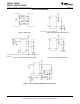
MECHANICAL DATA NFH0020A N0020A N20A (Rev G) www.ti.
IMPORTANT NOTICE Texas Instruments Incorporated and its subsidiaries (TI) reserve the right to make corrections, enhancements, improvements and other changes to its semiconductor products and services per JESD46, latest issue, and to discontinue any product or service per JESD48, latest issue. Buyers should obtain the latest relevant information before placing orders and should verify that such information is current and complete.