
Datasheet
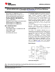


ADC0808-N, ADC0809-N
www.ti.com
SNAS535H –OCTOBER 1999–REVISED MARCH 2013
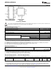
Electrical Characteristics – Converter Specifications (continued)
Converter Specifications: V
CC
=5 V
DC
=V
REF+
, V
REF(−)
=GND, T
MIN
≤T
A
≤T
MAX
and f
CLK
=640 kHz unless otherwise stated.
Symbol Parameter Conditions Min Typ Max Units
ADC0809
0°C to 70°C ±1 LSB
Total Unadjusted Error
(1)
T
MIN
to T
MAX
±1¼ LSB
Input Resistance From Ref(+) to Ref(−) 1.0 2.5 kΩ
Analog Input Voltage Range See
(2)
V(+) or V(−) GND − 0.1 V
CC
+ 0.1 V
DC
V
REF(+)
Voltage, Top of Ladder Measured at Ref(+) V
CC
V
CC
+ 0.1 V
Voltage, Center of Ladder (V
CC
/2) − 0.1 V
CC
/2 (V
CC
/2) + 0.1 V
V
REF(−)
Voltage, Bottom of Ladder Measured at Ref(−) −0.1 0 V
I
IN
Comparator Input Current f
c
=640 kHz,
(3)
−2 ±0.5 2 μA
(2) Two on-chip diodes are tied to each analog input which will forward conduct for analog input voltages one diode drop below ground or
one diode drop greater than the V
CC
n supply. The spec allows 100 mV forward bias of either diode. This means that as long as the
analog V
IN
does not exceed the supply voltage by more than 100 mV, the output code will be correct. To achieve an absolute 0V
DC
to
5V
DC
input voltage range will therefore require a minimum supply voltage of 4.900 V
DC
over temperature variations, initial tolerance and
loading.
(3) Comparator input current is a bias current into or out of the chopper stabilized comparator. The bias current varies directly with clock
frequency and has little temperature dependence (Figure 8). See ANALOG COMPARATOR INPUTS
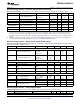
Electrical Characteristics – Digital Levels and DC Specifications
Digital Levels and DC Specifications: ADC0808CCN, ADC0808CCV, ADC0809CCN and ADC0809CCV, 4.75≤V
CC
≤5.25V,
−40°C≤T
A
≤+85°C unless otherwise noted
Symbol Parameter Conditions Min Typ Max Units
ANALOG MULTIPLEXER
V
CC
=5V, V
IN
=5V,
I
OFF(+)
OFF Channel Leakage Current T
A
=25°C 10 200 nA
T
MIN
to T
MAX
1.0 μA
V
CC
=5V, V
IN
=0,
I
OFF(−)
OFF Channel Leakage Current T
A
=25°C −200 −10 nA
T
MIN
to T
MAX
−1.0 μA
CONTROL INPUTS
V
IN(1)
Logical “1” Input Voltage (V
CC
− 1.5) V
V
IN(0)
Logical “0” Input Voltage 1.5 V
Logical “1” Input Current (The Control
I
IN(1)
V
IN
=15V 1.0 μA
Inputs)
Logical “0” Input Current (The Control
I
IN(0)
V
IN
=0 −1.0 μA
Inputs)
I
CC
Supply Current f
CLK
=640 kHz 0.3 3.0 mA
DATA OUTPUTS AND EOC (INTERRUPT)
V
CC
= 4.75V
V
OUT(1)
Logical “1” Output Voltage I
OUT
= −360µA 2.4 V
I
OUT
= −10µA 4.5 V
V
OUT(0)
Logical “0” Output Voltage I
O
=1.6 mA 0.45 V
V
OUT(0)
Logical “0” Output Voltage EOC I
O
=1.2 mA 0.45 V
V
O
=5V 3 μA
I
OUT
TRI-STATE Output Current
V
O
=0 −3 μA
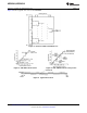
Electrical Characteristics – Timing Specifications
Timing Specifications V
CC
=V
REF(+)
=5V, V
REF(−)
=GND, t
r
=t
f
=20 ns and T
A
=25°C unless otherwise noted.
Symbol Parameter Conditions MIn Typ Max Units
t
STCLK
Start Time Delay from Clock (Figure 7) 300 900 ns
Copyright © 1999–2013, Texas Instruments Incorporated Submit Documentation Feedback 3
Product Folder Links: ADC0808-N ADC0809-N