
Datasheet
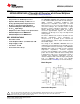


ADC0808-N, ADC0809-N
SNAS535H –OCTOBER 1999–REVISED MARCH 2013
www.ti.com
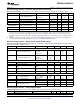
Electrical Characteristics – Timing Specifications (continued)
Timing Specifications V
CC
=V
REF(+)
=5V, V
REF(−)
=GND, t
r
=t
f
=20 ns and T
A
=25°C unless otherwise noted.
Symbol Parameter Conditions MIn Typ Max Units
t
WS
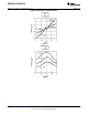
Minimum Start Pulse Width (Figure 7) 100 200 ns
t
WALE
Minimum ALE Pulse Width (Figure 7) 100 200 ns
t
s
Minimum Address Set-Up Time (Figure 7) 25 50 ns
t
H
Minimum Address Hold Time (Figure 7) 25 50 ns
t
D
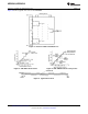
Analog MUX Delay Time From ALE R
S
=0Ω (Figure 7) 1 2.5 μs
t
H1
, t
H0
OE Control to Q Logic State C
L
=50 pF, R
L
=10k (Figure 10) 125 250 ns
t
1H
, t
0H
OE Control to Hi-Z C
L
=10 pF, R
L
=10k (Figure 10) 125 250 ns
t
c
Conversion Time f
c
=640 kHz, (Figure 7)
(1)
90 100 116 μs
f
c
Clock Frequency 10 640 1280 kHz
Clock
t
EOC
EOC Delay Time (Figure 7) 0 8 + 2 μS
Periods
C
IN
Input Capacitance At Control Inputs 10 15 pF
C
OUT
TRI-STATE Output Capacitance At TRI-STATE Outputs 10 15 pF
(1) The outputs of the data register are updated one clock cycle before the rising edge of EOC.
4 Submit Documentation Feedback Copyright © 1999–2013, Texas Instruments Incorporated
Product Folder Links: ADC0808-N ADC0809-N