
Datasheet

ADC0808-N, ADC0809-N
SNAS535H –OCTOBER 1999–REVISED MARCH 2013
www.ti.com
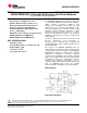
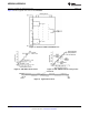
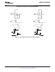
Figure 1. PDIP Package Figure 2. PLCC
Package
See Package N0028E
See Package FN0028A
These devices have limited built-in ESD protection. The leads should be shorted together or the device placed in conductive foam
during storage or handling to prevent electrostatic damage to the MOS gates.
Absolute Maximum Ratings
(1)(2)(3)
Supply Voltage (V
CC
)
(4)
6.5V
Voltage at Any Pin Except Control Inputs −0.3V to (V
CC
+0.3V)
Voltage at Control Inputs −0.3V to +15V
(START, OE, CLOCK, ALE, ADD A, ADD B, ADD C)
Storage Temperature Range −65°C to +150°C
Package Dissipation at T
A
=25°C 875 mW
Lead Temp. (Soldering, 10 seconds) PDIP Package (plastic) 260°C
PLCC Package Vapor Phase (60 seconds) 215°C
Infrared (15 seconds) 220°C
ESD Susceptibility
(5)
400V
(1) Absolute Maximum Ratings indicate limits beyond which damage to the device may occur. DC and AC electrical specifications do not
apply when operating the device beyond its specified operating conditions.
(2) All voltages are measured with respect to GND, unless otherwise specified.
(3) If Military/Aerospace specified devices are required, please contact the TI Sales Office/Distributors for availability and specifications.
(4) A Zener diode exists, internally, from V
CC
to GND and has a typical breakdown voltage of 7 V
DC
.
(5) Human body model, 100 pF discharged through a 1.5 kΩ resistor.
Operating Conditions
(1)(2)
Temperature Range T
MIN
≤T
A
≤T
MAX
−40°C≤T
A
≤+85°C
Range of V
CC
4.5 V
DC
to 6.0 V
DC
(1) Absolute Maximum Ratings indicate limits beyond which damage to the device may occur. DC and AC electrical specifications do not
apply when operating the device beyond its specified operating conditions.
(2) All voltages are measured with respect to GND, unless otherwise specified.
Electrical Characteristics – Converter Specifications
Converter Specifications: V
CC
=5 V
DC
=V
REF+
, V
REF(−)
=GND, T
MIN
≤T
A
≤T
MAX
and f
CLK
=640 kHz unless otherwise stated.
Symbol Parameter Conditions Min Typ Max Units
ADC0808
25°C ±½ LSB
Total Unadjusted Error
(1)
T
MIN
to T
MAX
±¾ LSB
(1) Total unadjusted error includes offset, full-scale, linearity, and multiplexer errors. See Figure 5. None of these A/Ds requires a zero or
full-scale adjust. However, if an all zero code is desired for an analog input other than 0.0V, or if a narrow full-scale span exists (for
example: 0.5V to 4.5V full-scale) the reference voltages can be adjusted to achieve this. See Figure 15.
2 Submit Documentation Feedback Copyright © 1999–2013, Texas Instruments Incorporated
Product Folder Links: ADC0808-N ADC0809-N