
Datasheet

ADC0808-N, ADC0809-N
www.ti.com
SNAS535H –OCTOBER 1999–REVISED MARCH 2013
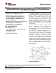
Functional Description
MULTIPLEXER
The device contains an 8-channel single-ended analog signal multiplexer. A particular input channel is selected
by using the address decoder. Table 1 shows the input states for the address lines to select any channel. The
address is latched into the decoder on the low-to-high transition of the address latch enable signal.
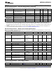
Table 1. Analog Channel Selection
ADDRESS LINE
SELECTED ANALOG
CHANNEL
C B A
IN0 L L L
IN1 L L H
IN2 L H L
IN3 L H H
IN4 H L L
IN5 H L H
IN6 H H L
IN7 H H H
CONVERTER CHARACTERISTICS
The Converter
The heart of this single chip data acquisition system is its 8-bit analog-to-digital converter. The converter is
designed to give fast, accurate, and repeatable conversions over a wide range of temperatures. The converter is
partitioned into 3 major sections: the 256R ladder network, the successive approximation register, and the
comparator. The converter's digital outputs are positive true.
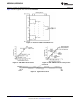
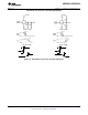
The 256R ladder network approach (Figure 3) was chosen over the conventional R/2R ladder because of its
inherent monotonicity, which ensures no missing digital codes. Monotonicity is particularly important in closed
loop feedback control systems. A non-monotonic relationship can cause oscillations that will be catastrophic for
the system. Additionally, the 256R network does not cause load variations on the reference voltage.
The bottom resistor and the top resistor of the ladder network in Figure 3 are not the same value as the
remainder of the network. The difference in these resistors causes the output characteristic to be symmetrical
with the zero and full-scale points of the transfer curve. The first output transition occurs when the analog signal
has reached +½ LSB and succeeding output transitions occur every 1 LSB later up to full-scale.
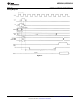
The successive approximation register (SAR) performs 8 iterations to approximate the input voltage. For any
SAR type converter, n-iterations are required for an n-bit converter. Figure 4 shows a typical example of a 3-bit
converter. In the ADC0808, ADC0809, the approximation technique is extended to 8 bits using the 256R
network.
The A/D converter's successive approximation register (SAR) is reset on the positive edge of the start conversion
start pulse. The conversion is begun on the falling edge of the start conversion pulse. A conversion in process
will be interrupted by receipt of a new start conversion pulse. Continuous conversion may be accomplished by
tying the end-of-conversion (EOC) output to the SC input. If used in this mode, an external start conversion pulse
should be applied after power up. End-of-conversion will go low between 0 and 8 clock pulses after the rising
edge of start conversion.
The most important section of the A/D converter is the comparator. It is this section which is responsible for the
ultimate accuracy of the entire converter. It is also the comparator drift which has the greatest influence on the
repeatability of the device. A chopper-stabilized comparator provides the most effective method of satisfying all
the converter requirements.
The chopper-stabilized comparator converts the DC input signal into an AC signal. This signal is then fed through
a high gain AC amplifier and has the DC level restored. This technique limits the drift component of the amplifier
since the drift is a DC component which is not passed by the AC amplifier. This makes the entire A/D converter
extremely insensitive to temperature, long term drift and input offset errors.
Copyright © 1999–2013, Texas Instruments Incorporated Submit Documentation Feedback 5
Product Folder Links: ADC0808-N ADC0809-N