
Datasheet

ADC0816, ADC0817
www.ti.com
SNAS527C –JUNE 1999–REVISED MARCH 2013
ADC0816/ADC0817 8-Bit μP Compatible A/D Converters
with16-Channel Multiplexer
Check for Samples: ADC0816, ADC0817
1
FEATURES
23
• Easy interface to all microprocessors
DESCRIPTION
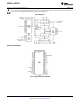
The ADC0816, ADC0817 data acquisition component
• Operates ratiometrically or with 5 V
DC
or
is a monolithic CMOS device with an 8-bit analog-to-
analog span adjusted voltage reference
digital converter,16-channel multiplexer and
• 16-channel multiplexer with latched control
microprocessor compatible control logic. The 8-bit
logic
A/D converter uses successive approximation as the
• Outputs meet TTL voltage level specifications
conversion technique. The converter features a high
impedance chopper stabilized comparator, a 256R
• 0V to 5V analog input voltage range with
voltage divider with analog switch tree and a
single 5V supply
successive approximation register. The 16-channel
• No zero or full-scale adjust required
multiplexer can directly access any one of 16-single-
• Standard hermetic or molded 40-pin MDIP
ended analog signals, and provides the logic for
package additional channel expansion. Signal conditioning of
any analog input signal is eased by direct access to
• Temperature range −40°C to +85°Cor −55°C to
the multiplexer output, and to the input of the 8-bit
+125°C
A/D converter.
• Latched TRI-STATE output
The device eliminates the need for external zero and
• Direct access to “comparator in” and
full-scale adjustments. Easy interfacing to
“multiplexer out” for signal conditioning
microprocessors is provided by the latched and
• ADC0816 equivalent to MM74C948
decoded multiplexer address inputs and latched TTL
TRI-STATE
®
outputs.
• ADC0817 equivalent to MM74C948-1
The design of the ADC0816, ADC0817 has been
KEY SPECIFICATIONS
optimized by incorporating the most desirable aspects
of several A/D conversion techniques. The
• Resolution ........................8 Bits
ADC0816,ADC0817 offers high speed, high
• Total Unadjusted Error....±½ LSB and ±1
accuracy, minimal temperature dependence,
• Single Supply....................5 V
DC
excellent long-term accuracy and repeatability, and
consumes minima lpower. These features make this
• Low Power........................15 mW
device ideally suited to applications from process and
• Conversion Time..............100 µs
machine control to consumer and automotive
applications. For similar performance in an 8-channel,
28-pin, 8-bit A/D converter, see the ADC0808,
ADC0809 data sheet. (See AN-258 for more
information.)
1
Please be aware that an important notice concerning availability, standard warranty, and use in critical applications of
Texas Instruments semiconductor products and disclaimers thereto appears at the end of this data sheet.
2TRI-STATE is a registered trademark of Texas Instruments.
3All other trademarks are the property of their respective owners.
PRODUCTION DATA information is current as of publication date.
Copyright © 1999–2013, Texas Instruments Incorporated
Products conform to specifications per the terms of the Texas
Instruments standard warranty. Production processing does not
necessarily include testing of all parameters.