
Datasheet

ADC0816, ADC0817
SNAS527C –JUNE 1999–REVISED MARCH 2013
www.ti.com
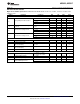
Electrical Characteristics
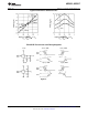
Timing Specifications:V
CC
= V
REF(+)
= 5V, V
REF(−)
= GND, t
r
= t
f
= 20 ns and T
A
= 25°C unless otherwise noted.
Symbol Parameter Conditions Min Typ Max Units
t
WS
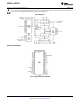
Minimum Start Pulse Width (Figure 5)
(1)
100 200 ns
t
WALE
Minimum ALE Pulse Width (Figure 5) 100 200 ns
t
s
Minimum Address Set-Up Time (Figure 5) 25 50 ns
T
H
Minimum Address Hold Time (Figure 5) 25 50 ns
Analog MUX Delay Time
t
D
R
S
= OΩ (Figure 5) 1 2.5 μs
from ALE
t
H1
, t
H0
OE Control to Q Logic State C
L
= 50 pF, R
L
= 10k (Figure 8) 125 250 ns
t
1H,
t
0H
OE Control to Hi-Z C
L
= 10 pF, R
L
= 10k (Figure 8) 125 250 ns
t
C
Conversion Time f
c
=640 kHz, (Figure 5)
(2)
90 100 116 μs
f
c
Clock Frequency 10 640 1280 kHz
Clock
t
EOC
EOC Delay Time (Figure 5) 0 8 + 2μs
Periods
C
IN
Input Capacitance At Control Inputs 10 15 pF
TRI-STATE Output
C
OUT
At TRI-STATE Outputs
(2)
10 15 pF
Capacitance
(1) If start pulse is asynchronous with converter clock or if f
c
> 640 kHz, the minimum start pulse width is 8clock periods plus 2 μs. For
synchronous operation at f
c
≤640 kHz take start high within 100 ns of clock going low.
(2) The outputs of the data register are updated one clock cycle before the rising edge of EOC.
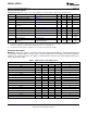
Functional Description
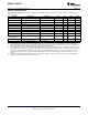
Multiplexer: The device contains a 16-channel single-ended analog signal multiplexer. A particular input channel
is selected by using the address decoder. Table 1 shows the input states for the address line and the expansion
control line to select any channel. The address is latched into the decoder on the low-to-high transition of the
address latch enable signal.
Table 1. Inputs States for the Address line
Selected Address Line
(1)
Expansion
AnalogChannel D C B A Control
IN0 L L L L H
IN1 L L L H H
IN2 L L H L H
IN3 L L H H H
IN4 L H L L H
IN5 L H L H H
IN6 L H H L H
IN7 L H H H H
IN8 H L L L H
IN9 H L L H H
IN10 H L H L H
IN11 H L H H H
IN12 H H L L H
IN13 H H L H H
IN14 H H H L H
IN15 H H H H H
All Channels OFF X X X X L
(1) X = don't care
6 Submit Documentation Feedback Copyright © 1999–2013, Texas Instruments Incorporated
Product Folder Links: ADC0816 ADC0817