
Datasheet
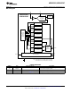
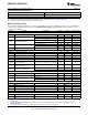
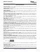

SDA
SCL
Lowest Conversion
Configuration
I
2
C Serial Interface
ADC081C021/
ADC081C027
Conversion Result
High Limit
Low Limit
Pointer
Register
and
Decode
Logic
Alert
Set-Point
Comparator
ADDR*
Highest Conversion
8-Bit
Successive
Approximation
ADC
GND
V
A
Hysteresis
V
IN
Alert Status
ALERT*
T/H
Oscillator
REF
* Note: The ADC081C021 has the ALERT pin but no ADDR pin.
The ADC081C027 has the ADDR pin but no ALERT pin.
ADC081C021, ADC081C027
www.ti.com
SNAS447C –FEBRUARY 2008–REVISED MARCH 2013
Block Diagram
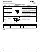
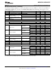
PIN DESCRIPTIONS
Symbol Type Equivalent Circuit Description
Power and unbufferred reference voltage. V
A
must be free
V
A
Supply
of noise and decoupled to GND.
GND Ground Ground for all on-chip circuitry.
V
IN
Analog Input See Figure 22 Analog input. This signal can range from GND to V
A
.
Copyright © 2008–2013, Texas Instruments Incorporated Submit Documentation Feedback 3
Product Folder Links: ADC081C021 ADC081C027