
Datasheet


I/O
GND
TO INTERNAL
CIRCUITRY
ADC081C021, ADC081C027
www.ti.com
SNAS447C –FEBRUARY 2008–REVISED MARCH 2013
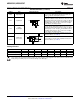
Absolute Maximum Ratings
(1)(2)(3)
Supply Voltage, V
A
(4)
-0.3V to +6.5V
Voltage on any Analog Input Pin to GND −0.3V to (V
A
+0.3V)
Voltage on any Digital Input Pin to GND −0.3V to 6.5V
Input Current at Any Pin
(5)
±15 mA
Package Input Current
(5)
±20 mA
Power Dissipation at T
A
= 25°C See
(6)
Human Body Model 2500V
VA, GND, V
IN
, ALERT, ADR pins Machine Model 250V
ESD Susceptibility
(7)
Charged Device Model (CDM) 1250V
Human Body Model 8000V
SDA, SCL pins
Machine Model 400V
Junction Temperature +150°C
Storage Temperature −65°C to +150°C
(1) Absolute Maximum Ratings indicate limits beyond which damage to the device may occur. Operating Ratings indicate conditions for
which the device is functional, but do not ensure specific performance limits. For ensured specifications and test conditions, see the
Electrical Characteristics. The ensured specifications apply only for the test conditions listed. Some performance characteristics may
degrade when the device is not operated under the listed test conditions. Operation of the device beyond the maximum Operating
Ratings is not recommended.
(2) All voltages are measured with respect to GND = 0V, unless otherwise specified.
(3) If Military/Aerospace specified devices are required, please contact the Texas Instruments Sales Office/Distributors for availability and
specifications.
(4) To ensure accuracy, it is required that V
A
be well bypassed and free of noise.
(5) When the input voltage at any pin exceeds 5.5V or is less than GND, the current at that pin should be limited per the Absolute Maximum
Ratings. The maximum package input current rating limits the number of pins that can safely exceed the power supplies.
(6) The absolute maximum junction temperature (T
J
max) for this device is 150°C. The maximum allowable power dissipation is dictated by
T
J
max, the junction-to-ambient thermal resistance (θ
JA
), and the ambient temperature (T
A
), and can be calculated using the formula
P
D
MAX = (T
J
max − T
A
) / θ
JA
. The values for maximum power dissipation will be reached only when the device is operated in a severe
fault condition (e.g., when input or output pins are driven beyond the operating ratings, or the power supply polarity is reversed).
(7) Human body model is a 100 pF capacitor discharged through a 1.5 kΩ resistor. Machine model is a 220 pF capacitor discharged
through 0 Ω. Charged device model simulates a pin slowly acquiring charge (such as from a device sliding down the feeder in an
automated assembler) then rapidly being discharged.
Operating Ratings
(1)(2)
Operating Temperature Range −40°C ≤ T
A
≤ +105°C
Supply Voltage, V
A
+2.7V to 5.5V
Analog Input Voltage, V
IN
0V to V
A
Digital Input Voltage
(3)
0V to 5.5V
Sample Rate up to 188.9 ksps
(1) Absolute Maximum Ratings indicate limits beyond which damage to the device may occur. Operating Ratings indicate conditions for
which the device is functional, but do not ensure specific performance limits. For ensured specifications and test conditions, see the
Electrical Characteristics. The ensured specifications apply only for the test conditions listed. Some performance characteristics may
degrade when the device is not operated under the listed test conditions. Operation of the device beyond the maximum Operating
Ratings is not recommended.
(2) All voltages are measured with respect to GND = 0V, unless otherwise specified.
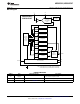
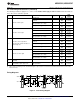
(3) The inputs are protected as shown below. Input voltage magnitudes up to 5.5V, regardless of V
A
, will not cause errors in the conversion
result. For example, if V
A
is 3V, the digital input pins can be driven with a 5V logic device.
Copyright © 2008–2013, Texas Instruments Incorporated Submit Documentation Feedback 5
Product Folder Links: ADC081C021 ADC081C027