
Datasheet


ADC081C021, ADC081C027
SNAS447C –FEBRUARY 2008–REVISED MARCH 2013
www.ti.com
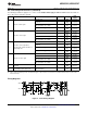
Package Thermal Resistances
(1)(2)
Package θ
JA
6-Lead SOT 250°C/W
8-Lead VSSOP 200°C/W
(1) Soldering process must comply with Reflow Temperature Profile specifications. Refer to www.ti.com/packaging.
(2) Reflow temperature profiles are different for lead-free packages.
Electrical Characteristics
The following specifications apply for V
A
= +2.7V to +5.5V, GND = 0V, f
SCL
up to 3.4MHz, f
IN
= 1kHz for f
SCL
up to 400kHz, f
IN
= 10kHz for f
SCL
= 3.4MHz unless otherwise noted. Boldface limits apply for T
A
= T
MIN
to T
MAX
: all other limits T
A
= 25°C
unless otherwise noted.
Symbol Parameter Conditions Typical
(1)
Limits
(1)
Units (Limits)
STATIC CONVERTER CHARACTERISTICS
Resolution with No Missing Codes 8 Bits
V
A
= +2.7V to +3.6V ±0.04 ±0.2 LSB (max)
Integral Non-Linearity (End Point
INL
Method)
V
A
= +2.7V to +5.5V. f
SCL
up to 400kHz
(2)
±0.1 ±0.25 LSB (max)
V
A
= +2.7V to +3.6V +0.04 ±0.2 LSB (max)
DNL Differential Non-Linearity
V
A
= +2.7V to +5.5V. f
SCL
up to 400kHz
(2)
±0.08 ±0.25 LSB (max)
V
A
= +2.7V to +3.6V +0.26 ±0.5 LSB (max)
V
OFF
Offset Error
V
A
= +2.7V to +5.5V. f
SCL
up to 400kHz
(2)
+0.25 ±0.5 LSB (max)
GE Gain Error -0.01 ±0.4 LSB (max)
DYNAMIC CONVERTER CHARACTERISTICS
ENOB Effective Number of Bits 7.98 7.8 Bits (min)
SNR Signal-to-Noise Ratio 49.8 49 dB (min)
THD Total Harmonic Distortion −70.6 −64 dB (max)
SINAD Signal-to-Noise Plus Distortion Ratio 49.8 49 dB (min)
SFDR Spurious-Free Dynamic Range -68.8 65 dB (min)
Intermodulation Distortion, Second
IMD V
A
= +3.0V, f
a
= 1.035 kHz, f
b
= 1.135 kHz −75.5 dB
Order Terms (IMD
2
)
Intermodulation Distortion, Third
V
A
= +3.0V, f
a
= 1.035 kHz, f
b
= 1.135 kHz −71.8 dB
Order Terms (IMD
3
)
V
A
= +3.0V 8 MHz
FPBW Full Power Bandwidth (−3dB)
V
A
= +5.0V 11 MHz
ANALOG INPUT CHARACTERISTICS
V
IN
Input Range 0 to V
A
V
I
DCL
DC Leakage Current
(3)
±1 µA (max)
Track Mode 30 pF
C
INA
Input Capacitance
Hold Mode 3 pF
SERIAL INTERFACE INPUT CHARACTERISTICS (SCL, SDA)
V
IH
Input High Voltage 0.7 x V
A
V (min)
V
IL
Input Low Voltage 0.3 x V
A
V (max)
I
IN
Input Current
(3)
±1 µA (max)
C
IN
Input Pin Capacitance 3 pF
V
HYST
Input Hysteresis 0.1 x V
A
V (min)
ADDRESS SELECTION INPUT CHARACTERISTICS (ADDR)
V
IH
Input High Voltage V
A
- 0.5V V (min)
V
IL
Input Low Voltage 0.5 V (max)
(1) Typical figures are at T
J
= 25°C, and represent most likely parametric norms. Test limits are specified to AOQL (Average Outgoing
Quality Level).
(2) The ADC will meet Minimum/Maximum specifications for f
SCL
up to 3.4MHz and V
A
= 2.7V to 3.6V when operating in the QUIET
INTERFACE MODE.
(3) This parameter is specified by design and/or characterization and is not tested in production.
6 Submit Documentation Feedback Copyright © 2008–2013, Texas Instruments Incorporated
Product Folder Links: ADC081C021 ADC081C027