
Datasheet

Snap
Back
GND
D1
PIN
V+
2.1k
41.5k
41.5k
Snap
Back
GND
D1
PIN
ADC081C021, ADC081C027
SNAS447C –FEBRUARY 2008–REVISED MARCH 2013
www.ti.com
PIN DESCRIPTIONS (continued)
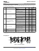
Symbol Type Equivalent Circuit Description
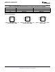
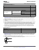
Alert output. Can be configured as active high or active low.
ALERT Digital Output This is an open drain data line that must be pulled to the
supply (V
A
) with an external pull-up resistor.
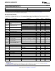
Serial Clock Input. SCL is used together with SDA to control
the transfer of data in and out of the device. This is an open
drain data line that must be pulled to the supply (V
A
) with an
SCL Digital Input
external pull-up resistor. This pin's extended ESD tolerance(
8kV HBM) allows extension of the I
2
C bus across multiple
boards without extra ESD protection.
Serial Data bi-directional connection. Data is clocked into or
out of the internal 16-bit register with SCL. This is an open
Digital drain data line that must be pulled to the supply (V
A
) with an
SDA
Input/Output external pull-up resistor. This pin's extended ESD tolerance(
8kV HBM) allows extension of the I
2
C bus across multiple
boards without extra ESD protection.
Tri-level Address Selection Input. Sets Bits A0 & A1 of the
ADDR0
7-bit slave address. (see Table 2)
Digital Input,
three levels
Tri-level Address Selection Input. Sets Bits A2 & A3 of the
ADDR1
7-bit slave address. (see Table 2)
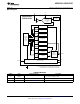
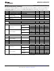
Package Pinouts
V
A
GND V
IN
ALERT SCL SDA ADR0 ADR1
ADC081C021 (SOT-6) 1 2 3 4 5 6 N/A N/A
ADC081C027 (SOT-6) 1 2 3 N/A 5 6 4 N/A
ADC081C021 (VSSOP-8) 5 7 4 2 1 8 3 6
These devices have limited built-in ESD protection. The leads should be shorted together or the device placed in conductive foam
during storage or handling to prevent electrostatic damage to the MOS gates.
4 Submit Documentation Feedback Copyright © 2008–2013, Texas Instruments Incorporated
Product Folder Links: ADC081C021 ADC081C027