
Datasheet
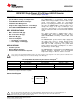


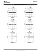

T/H
8-BIT
SUCCESSIVE
APPROXIMATION
ADC
SCLK
CS
SDATA
CONTROL
LOGIC
V
IN
ADC081S021
SNAS308E –APRIL 2005–REVISED MARCH 2013
www.ti.com
Block Diagram
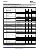
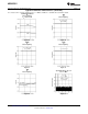
PIN DESCRIPTIONS AND EQUIVALENT CIRCUITS
Pin No. Symbol Description
ANALOG I/O
3 V
IN
Analog input. This signal can range from 0V to V
A
.
DIGITAL I/O
4 SCLK Digital clock input. This clock directly controls the conversion and readout processes.
5 SDATA Digital data output. The output samples are clocked out of this pin on falling edges of the SCLK pin.
6 CS Chip select. On the falling edge of CS, a conversion process begins.
POWER SUPPLY
Positive supply pin. This pin should be connected to a quiet +2.7V to +5.25V source and bypassed to
1 V
A
GND with a 1 µF capacitor and a 0.1 µF monolithic capacitor located within 1 cm of the power pin.
2 GND The ground return for the supply and signals.
PAD GND For package suffix CISD(X) only, it is recommended that the center pad should be connected to ground.
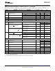
Absolute Maximum Ratings
(1)(2)(3)
Analog Supply Voltage V
A
−0.3V to 6.5V
Voltage on Any Analog Pin to GND −0.3V to (V
A
+0.3V)
Voltage on Any Digital Pin to GND −0.3V to 6.5V
Input Current at Any Pin
(4)
±10 mA
Package Input Current
(4)
±20 mA
Power Consumption at T
A
= 25°C See
(5)
ESD Susceptibility
(6)
Human Body Model 3500V
Machine Model 300V
Junction Temperature +150°C
Storage Temperature −65°C to +150°C
(1) Absolute Maximum Ratings indicate limits beyond which damage to the device may occur. Operating Ratings indicate conditions for
which the device is functional, but do not ensure specific performance limits. For ensured specifications and test conditions, see the
Electrical Characteristics. The ensured specifications apply only for the test conditions listed. Some performance characteristics may
degrade when the device is not operated under the listed test conditions.
(2) All voltages are measured with respect to GND = 0V, unless otherwise specified.
(3) If Military/Aerospace specified devices are required, please contact the TI Office/Distributors for availability and specifications.
(4) When the input voltage at any pin exceeds the power supply (that is, V
IN
< GND or V
IN
> V
A
), the current at that pin should be limited to
10 mA. The 20 mA maximum package input current rating limits the number of pins that can safely exceed the power supplies with an
input current of 10 mA to two. The Absolute Maximum Rating specification does not apply to the V
A
pin. The current into the V
A
pin is
limited by the Analog Supply Voltage specification.
(5) The absolute maximum junction temperature (T
J
max) for this device is 150°C. The maximum allowable power dissipation is dictated by
T
J
max, the junction-to-ambient thermal resistance (θ
JA
), and the ambient temperature (T
A
), and can be calculated using the formula
P
D
MAX = (T
J
max − T
A
)/θ
JA
. The values for maximum power dissipation listed above will be reached only when the device is operated in
a severe fault condition (e.g. when input or output pins are driven beyond the power supply voltages, or the power supply polarity is
reversed). Obviously, such conditions should always be avoided.
(6) Human body model is 100 pF capacitor discharged through a 1.5 kΩ resistor. Machine model is 220 pF discharged through zero ohms
2 Submit Documentation Feedback Copyright © 2005–2013, Texas Instruments Incorporated
Product Folder Links: ADC081S021