
Datasheet


ADC081S101
www.ti.com
SNAS310C –JANUARY 2006–REVISED MARCH 2013
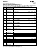
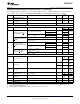
Absolute Maximum Ratings
(1)(2)(3)
Analog Supply Voltage V
A
−0.3V to 6.5V
Voltage on Any Pin to GND −0.3V to (V
A
+0.3)V
Input Current at Any Pin
(4)
±10 mA
Package Input Current
(4)
±20 mA
Power Consumption at T
A
= 25°C See
(5)
ESD Susceptibility
(6)
Human Body Model 3500V
Machine Model 300V
Junction Temperature +150°C
Storage Temperature −65°C to +150°C
(1) Absolute Maximum Ratings indicate limits beyond which damage to the device may occur. Operating Ratings indicate conditions for
which the device is functional, but do not ensure specific performance limits. For ensured specifications and test conditions, see the
Electrical Characteristics. The ensured specifications apply only for the test conditions listed. Some performance characteristics may
degrade when the device is not operated under the listed test conditions.
(2) If Military/Aerospace specified devices are required, please contact the Texas Instruments Sales Office/ Distributors for availability and
specifications.
(3) All voltages are measured with respect to GND = 0V, unless otherwise specified.
(4) When the input voltage at any pin exceeds the power supply (that is, V
IN
< GND or V
IN
> V
A
), the current at that pin should be limited to
10 mA. The 20 mA maximum package input current rating limits the number of pins that can safely exceed the power supplies with an
input current of 10 mA to two. The Absolute Maximum Rating specification does not apply to the V
A
pin. The current into the V
A
pin is
limited by the Analog Supply Voltage specification.
(5) The absolute maximum junction temperature (T
J
max) for this device is 150°C. The maximum allowable power dissipation is dictated by
T
J
max, the junction-to-ambient thermal resistance (θ
JA
), and the ambient temperature (T
A
), and can be calculated using the formula
P
D
max = (T
J
max − T
A
) / θ
JA
. The values for maximum power dissipation listed above will be reached only when the device is operated
in a severe fault condition (e.g. when input or output pins are driven beyond the power supply voltages, or the power supply polarity is
reversed). Obviously, such conditions should always be avoided.
(6) Human body model is 100 pF capacitor discharged through a 1.5 kΩ resistor. Machine model is 220 pF discharged through zero ohms.
Operating Ratings
(1)(2)
Operating Temperature Range −40°C ≤ T
A
≤ +85°C
V
A
Supply Voltage +2.7V to +5.25V
Digital Input Pins Voltage Range
−0.3V to +5.25V
(regardless of supply voltage)
Clock Frequency 25 kHz to 20 MHz
Sample Rate Up to 1 Msps
Analog Input Voltage 0V to V
A
(1) Absolute Maximum Ratings indicate limits beyond which damage to the device may occur. Operating Ratings indicate conditions for
which the device is functional, but do not ensure specific performance limits. For ensured specifications and test conditions, see the
Electrical Characteristics. The ensured specifications apply only for the test conditions listed. Some performance characteristics may
degrade when the device is not operated under the listed test conditions.
(2) All voltages are measured with respect to GND = 0V, unless otherwise specified.
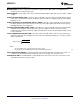
Package Thermal Resistance
(1)
Package θ
JA
6-lead WSON 94°C / W
6-lead SOT-23 265°C / W
Soldering process must comply with Texas Instrument's Reflow Temperature Profile specifications. Refer to www.ti.com and
http://www.ti.com/lit/SNOA549.
(1) Reflow temperature profiles are different for lead-free and non-lead-free packages.
Copyright © 2006–2013, Texas Instruments Incorporated Submit Documentation Feedback 3
Product Folder Links: ADC081S101