
Datasheet


ADC081S101
SNAS310C –JANUARY 2006–REVISED MARCH 2013
www.ti.com
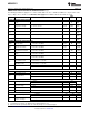
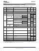
ADC081S101 Converter Electrical Characteristics
(1)(2)
The following specifications apply for V
A
= +2.7V to 5.25V, GND = 0V, f
SCLK
= 10 MHz to 20 MHz, C
L
= 15 pF, f
SAMPLE
= 500
ksps to 1 Msps, unless otherwise noted. Boldface limits apply for T
A
= T
MIN
to T
MAX
: all other limits T
A
= 25°C.
Limits
Symbol Parameter Conditions Typical Units
(2)
STATIC CONVERTER CHARACTERISTICS
Resolution with No Missing
8 Bits
Codes
LSB
INL Integral Non-Linearity V
A
= +2.7V to +5.25V ±0.05 ±0.3
(max)
LSB
DNL Differential Non-Linearity V
A
= +2.7V to +5.25V ±0.07 ±0.3
(max)
LSB
V
OFF
Offset Error V
A
= +2.7V to +5.25V ±0.03 ±0.3
(max)
LSB
GE Gain Error V
A
= +2.7V to +5.25V ±0.08 ±0.4
(max)
LSB
TUE Total Unadjusted Error V
A
= +2.7V to +5.25V ±0.07 ±0.3
(max)
DYNAMIC CONVERTER CHARACTERISTICS
Signal-to-Noise Plus V
A
= +2.7 to 5.25V
SINAD 49.7 49 dB (min)
Distortion Ratio f
IN
= 100 kHz, −0.02 dBFS
V
A
= +2.7 to 5.25V
SNR Signal-to-Noise Ratio 49.7 dB (min)
f
IN
= 100 kHz, −0.02 dBFS
V
A
= +2.7 to 5.25V
THD Total Harmonic Distortion −77 −65 dB (max)
f
IN
= 100 kHz, −0.02 dBFS
Spurious-Free Dynamic V
A
= +2.7 to 5.25V
SFDR 68 65 dB (min)
Range f
IN
= 100 kHz, −0.02 dBFS
V
A
= +2.7 to 5.25V
ENOB Effective Number of Bits 7.9 7.8 Bits (min)
f
IN
= 100 kHz, −0.02 dBFS
Intermodulation Distortion, V
A
= +5.25V
−68 dB
Second Order Terms f
a
= 103.5 kHz, f
b
= 113.5 kHz
IMD
Intermodulation Distortion, V
A
= +5.25V
−68 dB
Third Order Terms f
a
= 103.5 kHz, f
b
= 113.5 kHz
V
A
= +5V 11 MHz
FPBW -3 dB Full Power Bandwidth
V
A
= +3V 8 MHz
ANALOG INPUT CHARACTERISTICS
V
IN
Input Range 0 to V
A
V
I
DCL
DC Leakage Current ±1 µA (max)
Track Mode 30 pF
C
INA
Input Capacitance
Hold Mode 4 pF
DIGITAL INPUT CHARACTERISTICS
V
A
= +5.25V 2.4
V
IH
Input High Voltage V (min)
V
A
= +3.6V 2.1
V
A
= +5V 0.8 V (max)
V
IL
Input Low Voltage
V
A
= +3V 0.4 V (max)
I
IN
Input Current V
IN
= 0V or V
A
±10 nA ±1 µA (max)
C
IND
Digital Input Capacitance 2 4 pF (max)
DIGITAL OUTPUT CHARACTERISTICS
I
SOURCE
= 200 µA V
A
− 0.07 V
A
− 0.2 V (min)
V
OH
Output High Voltage
I
SOURCE
= 1 mA V
A
− 0.1 V
I
SINK
= 200 µA 0.03 0.4 V (max)
V
OL
Output Low Voltage
I
SINK
= 1 mA 0.1 V
(1) Tested limits are specified to TI's AOQL (Average Outgoing Quality Level).
(2) Data sheet min/max specification limits are ensured by design, test, or statistical analysis.
4 Submit Documentation Feedback Copyright © 2006–2013, Texas Instruments Incorporated
Product Folder Links: ADC081S101