
Datasheet


ADC081S101
www.ti.com
SNAS310C –JANUARY 2006–REVISED MARCH 2013
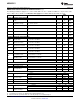
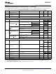
ADC081S101 Converter Electrical Characteristics
(1)(2)
(continued)
The following specifications apply for V
A
= +2.7V to 5.25V, GND = 0V, f
SCLK
= 10 MHz to 20 MHz, C
L
= 15 pF, f
SAMPLE
= 500
ksps to 1 Msps, unless otherwise noted. Boldface limits apply for T
A
= T
MIN
to T
MAX
: all other limits T
A
= 25°C.
Limits
Symbol Parameter Conditions Typical Units
(2)
TRI-STATE® Leakage
I
OZL
, I
OZH
±0.1 ±10 µA (max)
Current
TRI-STATE® Output
C
OUT
2 4 pF (max)
Capacitance
Output Coding Straight (Natural) Binary
POWER SUPPLY CHARACTERISTICS
2.7 V (min)
V
A
Supply Voltage
5.25 V (max)
SOT-23 3.2
mA
V
A
= +5.25V, f
SAMPLE
= 1 Msps 2.0
(max)
WSON 2.6
Supply Current, Normal
Mode (Operational, CS low)
SOT-23 1.5
mA
V
A
= +3.6V, f
SAMPLE
= 1 Msps 0.6
I
A
(max)
WSON 1.1
V
A
= +5.25V, f
SCLK
= 0 MHz, f
SAMPLE
= 0 ksps 500 nA
Supply Current, Shutdown
V
A
= +5.25V, f
SCLK
= 20 MHz,
(CS high)
60 µA
f
SAMPLE
= 0 ksps
SOT-23 16
mW
V
A
= +5V 10
Power Consumption,
(max)
WSON 13
Normal Mode (Operational,
SOT-23 4.5
mW
CS low)
V
A
= +3V 2.0
(max)
WSON 3.3
P
D
V
A
= +5V, f
SCLK
= 0 MHz,
2.5 µW
f
SAMPLE
= 0 ksps
Power Consumption,
Shutdown (CS high)
V
A
= +5V, f
SCLK
= 20 MHz,
300 µW
f
SAMPLE
= 0 ksps
AC ELECTRICAL CHARACTERISTICS
MHz
10
(min)
f
SCLK
Clock Frequency
(3)
MHz
20
(max)
ksps
50 500
(min)
f
S
Sample Rate
(3)
Msps
1
(max)
SCLk
t
HOLD
Hold Time 13 Falling
Edges
40 % (min)
DC SCLK Duty Cycle f
SCLK
= 20 MHz 50
60 % (max)
Minimum Time Required for
t
ACQ
350 ns (max)
Acquisition
t
QUIET
(4)
50 ns (min)
t
AD
Aperture Delay 3 ns
t
AJ
Aperture Jitter 30 ps
(3) This is the frequency range over which the electrical performance is ensured. The device is functional over a wider range which is
specified under Operating Ratings.
(4) Minimum Quiet Time required by bus relinquish and the start of the next conversion.
Copyright © 2006–2013, Texas Instruments Incorporated Submit Documentation Feedback 5
Product Folder Links: ADC081S101