
Datasheet

ADC0820-N
www.ti.com
SNAS529C –JUNE 1999–REVISED MARCH 2013
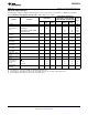
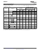
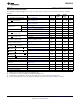
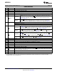
AC Electrical Characteristics
The following specifications apply for V
CC
= 5V, t
r
= t
f
= 20 ns, V
REF
(+) = 5V, V
REF
(−) = 0V and T
A
= 25°C unless otherwise
specified.
Tested Design
Parameter Conditions Typ
(1)
Units
Limit
(2)
Limit
(3)
t
CRD
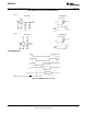
, Conversion Time for RD Mode Pin 7 = 0 (Figure 4) 1.6 2.5 µs
t
ACC0
, Access Time (Delay from Falling
Pin 7 = 0 (Figure 4) t
CRD
+ 20 t
CRD
+ 50 ns
Edge of RD to Output Valid)
t
CWR-RD
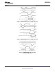
, Conversion Time for WR-RD Pin 7 = V
CC
; t
WR
= 600 ns, t
RD
=600 ns
1.52 µs
Mode (Figure 5 & Figure 6)
Min Pin 7 = V
CC
(Figure 5 & Figure 6) 600 ns
t
WR
, Write Time
Max Figure 11
(4)
50 µs
Pin 7 = V
CC
(Figure 5 & Figure 6 &
t
RD
, Read Time Min 600 ns
Figure 12)
(4)
Pin 7 = V
CC
, t
RD
< t
I
, C
L
= 15pF (Figure 5) 190 280 ns
t
ACC1
, Access Time (Delay from Falling
Edge of RD to Output Valid)
C
L
= 100 pF 210 320 ns
Pin 7 = V
CC
, t
RD
> t
I
, C
L
= 15pF (Figure 6) 70 120 ns
t
ACC2
, Access Time (Delay from Falling
Edge of RD to Output Valid)
C
L
=100 pF 90 150 ns
t
ACC3
, Access Time (Delay from Rising
R
PULLUP
= 1k and C
L
= 15 pF 30 ns
Edge of RDY to Output Valid)
Pin 7 = V
CC
, C
L
= 50pF (Figure 6 &
t
I
, Internal Comparison Time 800 1300 ns
Figure 7)
t
1H
, t
0H
, TRI-STATE Control (Delay from
R
L
= 1k, C
L
= 10 pF 100 200 ns
Rising Edge of RD to Hi-Z State)
Pin 7 = V
CC
, C
L
= 50 pF t
RD
> t
I
(Figure 6) t
I
ns
t
INTL
, Delay from Rising Edge of WR to
Falling Edge of INT
t
RD
< t
I
(Figure 5) t
RD
+200 t
RD
+290 ns
t
INTH
, Delay from Rising Edge of RD to C
L
= 50pF (Figure 4 & Figure 5 & Figure 6)
125 225 ns
Rising Edge of INT
t
INTHWR
, Delay from Rising Edge of WR to CL = 50pF (Figure 7)
175 270 ns
Rising Edge of INT
t
RDY
, Delay from CS to RDY C
L
= 50 pF, Pin 7 = 0 (Figure 4) 50 100 ns
t
ID
, Delay from INT to Output Valid See Figure 7 20 50 ns
t
RI
, Delay from RD to INT Pin 7 = V
CC
, t
RD
<t
I
Figure 5 200 290 ns
t
P
, Delay from End of Conversion to Next (Figure 4 & Figure 5 & Figure 6 & Figure 7
500 ns
Conversion & Figure 13)
(4)
Slew Rate, Tracking 0.1 V/µs
C
VIN
, Analog Input Capacitance 45 pF
C
OUT
, Logic Output Capacitance 5 pF
C
IN
, Logic Input Capacitance 5 pF
(1) Typicals are at 25°C and represent most likely parametric norm.
(2) Tested limits are ensured to TI's AOQL (Average Outgoing Quality Level).
(3) Design limits are specified but not 100% tested. These limits are not used to calculate outgoing quality levels.
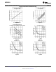
(4) Accuracy may degrade if t
WR
or t
RD
is shorter than the minimum value specified. See Figure 11 and Figure 12 graphs.
Copyright © 1999–2013, Texas Instruments Incorporated Submit Documentation Feedback 5
Product Folder Links: ADC0820-N