
Datasheet
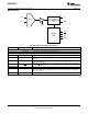
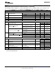
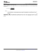

IN1
IN2
MUX
T/H
SCLK
V
A
GND
CS
DIN
DOUT
CONTROL
LOGIC
8-BIT
SUCCESSIVE
APPROXIMATION
ADC
GND
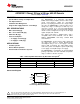
ADC082S051
SNAS263F –NOVEMBER 2004–REVISED MARCH 2013
www.ti.com
Block Diagram
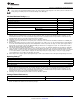
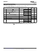
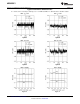
Pin Descriptions and Equivalent Circuits
Pin No. Pin Name Description
ANALOG I/O
5,4 IN1 and IN2 Analog inputs. These signals can range from 0V to V
A
.
DIGITAL I/O
8 SCLK Digital clock input. This clock directly controls the conversion and readout processes.
Digital data output. The output samples are clocked out of this pin on falling edges of the
7 DOUT
SCLK pin.
Digital data input. The ADC082S051's Control Register is loaded through this pin on rising
6 DIN
edges of the SCLK pin.
Chip select. On the falling edge of CS, a conversion process begins. Conversions continue
1 CS
as long as CS is held low.
POWER SUPPLY
Positive supply pin. This pin should be connected to a quiet +2.7V to +5.25V source and
2 V
A
bypassed to GND with a 1 µF capacitor and a 0.1 µF monolithic capacitor located within 1
cm of the power pin.
3 GND The ground return for the die.
2 Submit Documentation Feedback Copyright © 2004–2013, Texas Instruments Incorporated
Product Folder Links: ADC082S051