
Datasheet
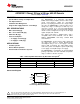

ADC082S051
www.ti.com
SNAS263F –NOVEMBER 2004–REVISED MARCH 2013
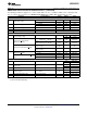
ADC082S051 Converter Electrical Characteristics
(1)
(continued)
The following specifications apply for V
A
= +2.7V to 5.25V, GND = 0V, f
SCLK
= 3.2 MHz to 8 MHz, f
SAMPLE
= 200 ksps to 500
ksps, C
L
= 50 pF, unless otherwise noted. Boldface limits apply for T
A
= T
MIN
to T
MAX
: all other limits T
A
= 25°C.
Parameter Test Conditions Typical Limits
(2)
Units
DIGITAL OUTPUT CHARACTERISTICS
I
SOURCE
= 200 µA V
A
− 0.03 V
A
− 0.5 V (min)
V
OH
Output High Voltage
I
SOURCE
= 1 mA V
A
− 0.1 V
I
SINK
= 200 µA 0.03 0.4 V (max)
V
OL
Output Low Voltage
I
SINK
= 1 mA 0.1 V
I
OZH
, I
OZL
TRI-STATE Leakage Current 0.005 ±1 µA (max)
C
OUT
TRI-STATE Output Capacitance 2 4 pF (max)
Output Coding Straight (Natural) Binary
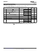
POWER SUPPLY CHARACTERISTICS (C
L
= 10 pF)
2.7 V (min)
V
A
Analog Supply Voltage
5.25 V (max)
V
A
= +5.25V,
1.35 1.9 mA (max)
f
SAMPLE
= 500 ksps, f
IN
= 40 kHz
Supply Current, Normal Mode
(Operational, CS low)
V
A
= +3.6V,
0.62 0.9 mA (max)
f
SAMPLE
= 500 ksps, f
IN
= 40 kHz
I
A
V
A
= +5.25V,
200 nA
f
SAMPLE
= 0 ksps
Supply Current, Shutdown (CS high)
V
A
= +3.6V,
200 nA
f
SAMPLE
= 0 ksps
V
A
= +5.25V 7.1 10 mW (max)
Power Consumption, Normal Mode
(Operational, CS low)
V
A
= +3.6V 2.23 3.2 mW (max)
P
D
V
A
= +5.25V 0.35 µW
Power Consumption, Shutdown (CS
high)
V
A
= +3.6V 0.12 µW
AC ELECTRICAL CHARACTERISTICS
3.2 MHz (min)
f
SCLK
Clock Frequency See
(3)
8 MHz (max)
200 ksps (min)
f
S
Sample Rate See
(3)
500 ksps (max)
t
CONV
Conversion Time 13 SCLK cycles
30 % (min)
DC SCLK Duty Cycle f
SCLK
= 8 MHz 50
70 % (max)
t
ACQ
Track/Hold Acquisition Time Full-Scale Step Input 3 SCLK cycles
Throughput Time Acquisition Time + Conversion Time 16 SCLK cycles
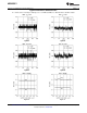
(3) This is the frequency range over which the electrical performance is specified. The device is functional over a wider range which is
specified under Operating Ratings.
Copyright © 2004–2013, Texas Instruments Incorporated Submit Documentation Feedback 5
Product Folder Links: ADC082S051