
Datasheet
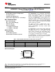

ADC082S051
SNAS263F –NOVEMBER 2004–REVISED MARCH 2013
www.ti.com
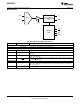
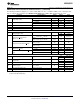
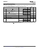
ADC082S051 Timing Specifications
The following specifications apply for V
A
= +2.7V to 5.25V, GND = 0V, f
SCLK
= 3.2 MHz to 8 MHz, f
SAMPLE
= 200 ksps to 500
ksps, C
L
= 50 pF, Boldface limits apply for T
A
= T
MIN
to T
MAX
: all other limits T
A
= 25°C.
Limits
Parameter Test Conditions Typical Units
(1)
V
A
= +3.0V −3.5
t
CSU
Setup Time SCLK High to CS Falling Edge See
(2)
10 ns (min)
V
A
= +5.0V −0.5
V
A
= +3.0V +4.5
t
CLH
Hold time SCLK Low to CS Falling Edge See
(2)
10 ns (min)
V
A
= +5.0V +1.5
V
A
= +3.0V +4
t
EN
Delay from CS Until DOUT active 30 ns (max)
V
A
= +5.0V +2
V
A
= +3.0V +16.5
t
ACC
Data Access Time after SCLK Falling Edge 30 ns (max)
V
A
= +5.0V +15
t
SU
Data Setup Time Prior to SCLK Rising Edge +3 10 ns (min)
t
H
Data Valid SCLK Hold Time +3 10 ns (min)
t
CH
SCLK High Pulse Width 0.5 x t
SCLK
0.3 x t
SCLK
ns (min)
t
CL
SCLK Low Pulse Width 0.5 x t
SCLK
0.3 x t
SCLK
ns (min)
V
A
= +3.0V 1.7
Output Falling
V
A
= +5.0V 1.2
t
DIS
CS Rising Edge to DOUT High-Impedance 20 ns (max)
V
A
= +3.0V 1.0
Output Rising
V
A
= +5.0V 1.0
(1) Tested limits are ensured to TI's AOQL (Average Outgoing Quality Level).
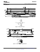
(2) Clock may be either high or low when CS is asserted as long as setup and hold times t
CSU
and t
CLH
are strictly observed.
6 Submit Documentation Feedback Copyright © 2004–2013, Texas Instruments Incorporated
Product Folder Links: ADC082S051