
Datasheet

t
CSU
t
CLH
SCLK
CS
SCLK
t
CONVERT
t
ACQ
t
CL
t
ACC
t
EN
Z3 Z2 Z1 Z0
DB6
DONT DONTC ADD2 ADD1 ADD0
DONTC
DONTC DONTC
DB7
DB5 DB4
DB0
16
87654321
DIN
DOUT
SCLK
CS
t
DIS
Zero ZeroDB1
151413
Tri-State
Zero Zero
1211
t
CH
t
H
t
SU
1 2 3 4 5 6 7 8 9 10 11 12 13 14 15 16
1 2 3 4 5 6 7 8
Track Hold
Power Up
Track Hold
b7 b6 b5 b4 b3 b2 b1 b0 b7 b6 b5 b4 b3 b2 b1 b0
9 10
DB5 DB4 DB3 DB2 DB1 DB0 DB5 DB4 DB3
DIN
DOUT
Power Up
SCLK
CS
Power Down
Control register
Control register
DB7 DB6
DB7 DB6
ADC082S051
www.ti.com
SNAS263F –NOVEMBER 2004–REVISED MARCH 2013
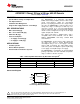
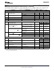
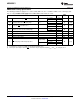
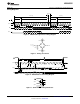
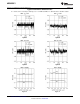
Timing Diagrams
Figure 2. ADC082S051 Operational Timing Diagram
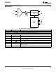
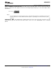
Figure 3. Timing Test Circuit
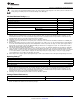
Figure 4. ADC082S051 Serial Timing Diagram
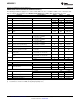
Figure 5. SCLK and CS Timing Parameters
Copyright © 2004–2013, Texas Instruments Incorporated Submit Documentation Feedback 7
Product Folder Links: ADC082S051