
Datasheet


ADC0831-N, ADC0832-N, ADC0834-N, ADC0838-N
SNAS531B –AUGUST 1999–REVISED MARCH 2013
www.ti.com
Adjusting for an Arbitrary Analog Input Voltage Range
If the analog zero voltage of the A/D is shifted away from ground (for example, to accommodate an analog input
signal which does not go to ground), this new zero reference should be properly adjusted first. A V
IN
(+) voltage
which equals this desired zero reference plus ½ LSB (where the LSB is calculated for the desired analog span,
using 1 LSB= analog span/256) is applied to selected “+” input and the zero reference voltage at the
corresponding “−” input should then be adjusted to just obtain the 00
HEX
to 01
HEX
code transition.
The full-scale adjustment should be made [with the proper V
IN
(−) voltage applied] by forcing a voltage to the
V
IN
(+) input which is given by:
where
• V
MAX
= the high end of the analog input range
• V
MIN
= the low end (the offset zero) of the analog range. (Both are ground referenced.) (2)
The V
REF
(or V
CC
) voltage is then adjusted to provide a code change from FE
HEX
to FF
HEX
. This completes the
adjustment procedure.
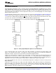
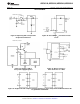
Power Supply
A unique feature of the ADC0838-N and ADC0834-N is the inclusion of a zener diode connected from the V
+
terminal to ground which also connects to the V
CC
terminal (which is the actual converter supply) through a
silicon diode, as shown in Figure 24
(1)
.
Figure 24. An On-Chip Shunt Regulator Diode
This zener is intended for use as a shunt voltage regulator to eliminate the need for any additional regulating
components. This is most desirable if the converter is to be remotely located from the system power source.
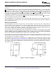
Figure 25 and Figure 27 illustrate two useful applications of this on-board zener when an external transistor can
be afforded.
An important use of the interconnecting diode between V
+
and V
CC
is shown in Figure 26 and Figure 28. Here,
this diode is used as a rectifier to allow the V
CC
supply for the converter to be derived from the clock. The low
current requirements of the A/D and the relatively high clock frequencies used (typically in the range of 10k–400
kHz) allows using the small value filter capacitor shown to keep the ripple on the V
CC
line to well under ¼ of an
LSB. The shunt zener regulator can also be used in this mode. This requires a clock voltage swing which is in
excess of V
Z
. A current limit for the zener is needed, either built into the clock generator or a resistor can be used
from the CLK pin to the V
+
pin.
(1) Internal zener diodes (6.3 to 8.5V) are connected from V+ to GND and V
CC
to GND. The zener at V+ can operate as a shunt regulator
and is connected to V
CC
via a conventional diode. Since the zener voltage equals the A/D's breakdown voltage, the diode insures that
V
CC
will be below breakdown when the device is powered from V+. Functionality is therefore ensured for V+ operation even though the
resultant voltage at V
CC
may exceed the specified Absolute Max of 6.5V. It is recommended that a resistor be used to limit the max
current into V+. (See Figure 24 in Functional Description)
18 Submit Documentation Feedback Copyright © 1999–2013, Texas Instruments Incorporated
Product Folder Links: ADC0831-N ADC0832-N ADC0834-N ADC0838-N