
Datasheet

ADC0831-N, ADC0832-N, ADC0834-N, ADC0838-N
SNAS531B –AUGUST 1999–REVISED MARCH 2013
www.ti.com
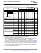
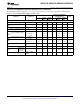
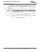
Converter and Multiplexer Electrical Characteristics
The following specifications apply for V
CC
= V+ = V
REF
= 5V, V
REF
≤ V
CC
+0.1V, T
A
= T
j
= 25°C, and f
CLK
= 250 kHz unless
otherwise specified. Boldface limits apply from T
MIN
to T
MAX
.
BCV, CCV, CCWM, BCN
CIWM Devices
and CCN Devices
Parameter Conditions Units
Tested Design Tested Design
Typ
(1)
Typ
(1)
Limit
(2)
Limit
(3)
Limit
(2)
Limit
(3)
CONVERTER AND MULTIPLEXER CHARACTERISTICS
ADC0838BCV ±½ ±½
ADC0834BCN ±½ ±½
Total
ADC0838CCV ±1 ±1
Unadjusted V
REF
= 5.00 V
(4)
LSB (Max)
ADC0831/2/4/8CCN ±1 ±1
Error
ADC0831/2/4/8CCWM ±1 ±1
ADC0832/8CIWM ±1
Minimum Reference Input
3.5 1.3 3.5 1.3 1.3 kΩ
Resistance
(5)
Maximum Reference Input
3.5 5.9 3.5 5.4 5.9 kΩ
Resistance
(5)
Maximum Common-Mode Input V
CC
V
CC
V
CC
+0.05 V
Range
(6)
+0.05 +0.05
Minimum Common-Mode Input GND GND GND
V
Range
(6)
−0.05 −0.05 −0.05
DC Common-Mode Error ±1/16 ±¼ ±1/16 ±¼ ±¼ LSB
15 mA into V+, V
CC
=
Change in zero error from V
CC
=5V
N.C., 1 1 1 LSB
to internal zener operation
(7)
V
REF
= 5V
V
Z
, internal diode MIN 15 mA into V+ 6.3 6.3 6.3
breakdown (at V+)
(7)
MAX 8.5 8.5 8.5 V
Power Supply Sensitivity V
CC
= 5V ± 5% ±1/16 ±¼ ±¼ ±1/16 ±¼ ±¼ LSB
On Channel = 5V −0.2 −0.2 −1 μA
Off Channel = 0V −1
I
OFF
, Off Channel Leakage
Current
(8)
On Channel = 0V +0.2 +0.2 +1 μA
Off Channel = 5V +1
On Channel = 0V −0.2 −0.2 −1 μA
Off Channel = 5V −1
I
ON
, On Channel Leakage Current
(8)
On Channel = 5V +0.2 +0.2 +1 μA
Off Channel = 0V +1
(1) Typicals are at 25°C and represent most likely parametric norm.
(2) Tested limits are ensured to TI's AOQL (Average Outgoing Quality Level).
(3) Ensured but not 100% production tested. These limits are not used to calculate outgoing quality levels.
(4) Total unadjusted error includes offset, full-scale, linearity, and multiplexer errors.
(5) Cannot be tested for ADC0832-N.
(6) For V
IN
(−) ≥ V
IN
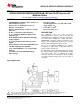
(+) the digital output code will be 0000 0000. Two on-chip diodes are tied to each analog input (see Functional Block
Diagram) which will forward conduct for analog input voltages one diode drop below ground or one diode drop greater than the V
CC
supply. Be careful, during testing at low V
CC
levels (4.5V), as high level analog inputs (5V) can cause this input diode to
conduct—especially at elevated temperatures, and cause errors for analog inputs near full-scale. The spec allows 50 mV forward bias of
either diode. This means that as long as the analog V
IN
or V
REF
does not exceed the supply voltage by more than 50 mV, the output
code will be correct. To achieve an absolute 0 V
DC
to 5 V
DC
input voltage range will therefore require a minimum supply voltage of 4.950
V
DC
over temperature variations, initial tolerance and loading.
(7) Internal zener diodes (6.3 to 8.5V) are connected from V+ to GND and V
CC
to GND. The zener at V+ can operate as a shunt regulator
and is connected to V
CC
via a conventional diode. Since the zener voltage equals the A/D's breakdown voltage, the diode insures that
V
CC
will be below breakdown when the device is powered from V+. Functionality is therefore ensured for V+ operation even though the
resultant voltage at V
CC
may exceed the specified Absolute Max of 6.5V. It is recommended that a resistor be used to limit the max
current into V+. (See Figure 24 in Functional Description)
(8) Leakage current is measured with the clock not switching.
4 Submit Documentation Feedback Copyright © 1999–2013, Texas Instruments Incorporated
Product Folder Links: ADC0831-N ADC0832-N ADC0834-N ADC0838-N