
Datasheet

ADC0831-N, ADC0832-N, ADC0834-N, ADC0838-N
SNAS531B –AUGUST 1999–REVISED MARCH 2013
www.ti.com
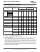
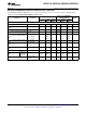
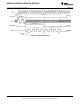
AC Characteristics
The following specifications apply for V
CC
= 5V, t
r
= t
f
= 20 ns and 25°C unless otherwise specified.
Tested Design Limit
Parameter Conditions Typ
(1)
Limit
(2)
Limit
(3)
Units
Min 10 kHz
f
CLK
, Clock Frequency
Max 400 kHz
t
C
, Conversion Time Not including MUX Addressing Time 8 1/f
CLK
Min 40 %
Clock Duty Cycle
(4)
Max 60 %
t
SET-UP
, CS Falling Edge or Data Input Valid
250 ns
to CLK Rising Edge
t
HOLD
, Data Input Valid after CLK Rising
90 ns
Edge
C
L
=100 pF
t
pd1
, t
pd0
—CLK Falling Edge to Output Data
Data MSB First 650 1500 ns
Valid
(5)
Data LSB First 250 600 ns
C
L
=10 pF, R
L
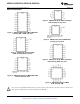
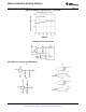
=10k (See TRI-STATE
125 250 ns
t
1H
, t
0H
,—Rising Edge of CS to Data Output
Test Circuits and Waveforms)
and SARS Hi–Z
C
L
=100 pf, R
L
=2k 500 ns
C
IN
, Capacitance of Logic Input 5 pF
C
OUT
, Capacitance of Logic Outputs 5 pF
(1) Typicals are at 25°C and represent most likely parametric norm.
(2) Tested limits are ensured to TI's AOQL (Average Outgoing Quality Level).
(3) Ensured but not 100% production tested. These limits are not used to calculate outgoing quality levels.
(4) A 40% to 60% clock duty cycle range insures proper operation at all clock frequencies. In the case that an available clock has a duty
cycle outside of these limits, the minimum, time the clock is high or the minimum time the clock is low must be at least 1 μs. The
maximum time the clock can be high is 60 μs. The clock can be stopped when low so long as the analog input voltage remains stable.
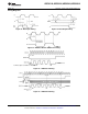
(5) Since data, MSB first, is the output of the comparator used in the successive approximation loop, an additional delay is built in (see
ADC0838-N Functional Block Diagram) to allow for comparator response time.
6 Submit Documentation Feedback Copyright © 1999–2013, Texas Instruments Incorporated
Product Folder Links: ADC0831-N ADC0832-N ADC0834-N ADC0838-N