
Datasheet


ADC0831-N, ADC0832-N, ADC0834-N, ADC0838-N
www.ti.com
SNAS531B –AUGUST 1999–REVISED MARCH 2013
THE DIGITAL INTERFACE
A most important characteristic of these converters is their serial data link with the controlling processor. Using a
serial communication format offers two very significant system improvements; it allows more function to be
included in the converter package with no increase in package size and it can eliminate the transmission of low
level analog signals by locating the converter right at the analog sensor; transmitting highly noise immune digital
data back to the host processor.
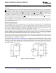
To understand the operation of these converters it is best to refer to the Timing Diagrams and Functional Block
Diagram and to follow a complete conversion sequence. For clarity a separate diagram is shown of each device.
1. A conversion is initiated by first pulling the CS (chip select) line low. This line must be held low for the entire
conversion. The converter is now waiting for a start bit and its MUX assignment word.
2. A clock is then generated by the processor (if not provided continuously) and output to the A/D clock input.
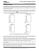
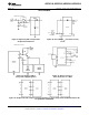
8 Single-Ended 8 Pseudo-Differential
4 Differential Mixed Mode
Figure 22. Analog Input Multiplexer Options for the ADC0838-N
3. On each rising edge of the clock the status of the data in (DI) line is clocked into the MUX address shift
register. The start bit is the first logic “1” that appears on this line (all leading zeros are ignored). Following the
start bit the converter expects the next 2 to 4 bits to be the MUX assignment word.
4. When the start bit has been shifted into the start location of the MUX register, the input channel has been
assigned and a conversion is about to begin. An interval of ½ clock period (where nothing happens) is
automatically inserted to allow the selected MUX channel to settle. The SAR status line goes high at this time to
signal that a conversion is now in progress and the DI line is disabled (it no longer accepts data).
5. The data out (DO) line now comes out of TRI-STATE and provides a leading zero for this one clock period of
MUX settling time.
6. When the conversion begins, the output of the SAR comparator, which indicates whether the analog input is
greater than (high) or less than (low) each successive voltage from the internal resistor ladder, appears at the
DO line on each falling edge of the clock. This data is the result of the conversion being shifted out (with the
MSB coming first) and can be read by the processor immediately.
Copyright © 1999–2013, Texas Instruments Incorporated Submit Documentation Feedback 15
Product Folder Links: ADC0831-N ADC0832-N ADC0834-N ADC0838-N