
Datasheet


ADC0831-N, ADC0832-N, ADC0834-N, ADC0838-N
SNAS531B –AUGUST 1999–REVISED MARCH 2013
www.ti.com
7. After 8 clock periods the conversion is completed. The SAR status line returns low to indicate this ½ clock
cycle later.
8. If the programmer prefers, the data can be provided in an LSB first format [this makes use of the shift enable
(SE) control line]. All 8 bits of the result are stored in an output shift register. On devices which do not include the
SE control line, the data, LSB first, is automatically shifted out the DO line, after the MSB first data stream. The
DO line then goes low and stays low until CS is returned high. On the ADC0838-N the SE line is brought out and
if held high, the value of the LSB remains valid on the DO line. When SE is forced low, the data is then clocked
out LSB first. The ADC0831-N is an exception in that its data is only output in MSB first format.
9. All internal registers are cleared when the CS line is high. If another conversion is desired, CS must make a
high to low transition followed by address information.
The DI and DO lines can be tied together and controlled through a bidirectional processor I/O bit with one wire.
This is possible because the DI input is only “looked-at” during the MUX addressing interval while the DO line is
still in a high impedance state.
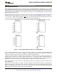
Reference Considerations
The voltage applied to the reference input to these converters defines the voltage span of the analog input (the
difference between V
IN(MAX)
and V
IN(MIN)
) over which the 256 possible output codes apply. The devices can be
used in either ratiometric applications or in systems requiring absolute accuracy. The reference pin must be
connected to a voltage source capable of driving the reference input resistance of typically 3.5 kΩ. This pin is the
top of a resistor divider string used for the successive approximation conversion.
In a ratiometric system, the analog input voltage is proportional to the voltage used for the A/D reference. This
voltage is typically the system power supply, so the V
REF
pin can be tied to V
CC
(done internally on the ADC0832-
N). This technique relaxes the stability requirements of the system reference as the analog input and A/D
reference move together maintaining the same output code for a given input condition.
For absolute accuracy, where the analog input varies between very specific voltage limits, the reference pin can
be biased with a time and temperature stable voltage source. The LM385 and LM336 reference diodes are good
low current devices to use with these converters.
The maximum value of the reference is limited to the V
CC
supply voltage. The minimum value, however, can be
quite small (see Typical Performance Characteristics) to allow direct conversions of transducer outputs providing
less than a 5V output span. Particular care must be taken with regard to noise pickup, circuit layout and system
error voltage sources when operating with a reduced span due to the increased sensitivity of the converter (1
LSB equals V
REF
/256).
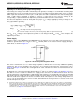
a) Ratiometric b) Absolute with a reduced Span
Figure 23. Reference Examples
16 Submit Documentation Feedback Copyright © 1999–2013, Texas Instruments Incorporated
Product Folder Links: ADC0831-N ADC0832-N ADC0834-N ADC0838-N