ADC0831-N, ADC0832-N, ADC0834-N, ADC0838-N www.ti.
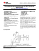
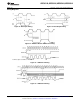
ADC0831-N, ADC0832-N, ADC0834-N, ADC0838-N SNAS531B – AUGUST 1999 – REVISED MARCH 2013 www.ti.com Connection Diagrams Figure 4. ADC0831-N Single Differential Input PDIP Package (P) Top View Figure 1. ADC0838-N 8-Channel Mux SOIC/PDIP Package (DW or NFH) Top View COM internally connected to GND. VREF internally connected to VCC. Top View Figure 5. ADC0832-N 2-Channel MUX PDIP Package (P) Top View Figure 2. ADC0832-N 2-Channel MUX SOIC Package (NPA) Top View Figure 6.
ADC0831-N, ADC0832-N, ADC0834-N, ADC0838-N www.ti.com SNAS531B – AUGUST 1999 – REVISED MARCH 2013 Absolute Maximum Ratings (1) (2) (3) Current into V+ (4) 15 mA Supply Voltage, VCC (4) 6.5V Voltage Logic Inputs −0.3V to VCC + 0.3V Analog Inputs −0.3V to VCC + 0.3V Pin Input Current per (5) ±5 mA Package ±20 mA −65°C to +150°C Storage Temperature Package Dissipation at TA = 25°C (Board Mount) Lead Temperature (Soldering 10 sec.) PDIP Package 260°C Vapor Phase (60 sec.
ADC0831-N, ADC0832-N, ADC0834-N, ADC0838-N SNAS531B – AUGUST 1999 – REVISED MARCH 2013 www.ti.com Converter and Multiplexer Electrical Characteristics The following specifications apply for VCC = V+ = VREF = 5V, VREF ≤ VCC +0.1V, TA = Tj = 25°C, and fCLK = 250 kHz unless otherwise specified. Boldface limits apply from TMIN to TMAX.
ADC0831-N, ADC0832-N, ADC0834-N, ADC0838-N www.ti.com SNAS531B – AUGUST 1999 – REVISED MARCH 2013 Converter and Multiplexer Electrical Characteristics (continued) The following specifications apply for VCC = V+ = VREF = 5V, VREF ≤ VCC +0.1V, TA = Tj = 25°C, and fCLK = 250 kHz unless otherwise specified. Boldface limits apply from TMIN to TMAX.
ADC0831-N, ADC0832-N, ADC0834-N, ADC0838-N SNAS531B – AUGUST 1999 – REVISED MARCH 2013 www.ti.com AC Characteristics The following specifications apply for VCC = 5V, tr = tf = 20 ns and 25°C unless otherwise specified.
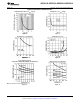
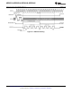
ADC0831-N, ADC0832-N, ADC0834-N, ADC0838-N www.ti.com SNAS531B – AUGUST 1999 – REVISED MARCH 2013 Typical Performance Characteristics Unadjusted Offset Error vs. VREF Voltage Linearity Error vs. VREFVoltage Figure 8. Figure 9. Linearity Error vs. Temperature Linearity Error vs. fCLK Figure 10. Figure 11. Power Supply Current vs. Temperature (ADC0838-N, ADC0831-N, ADC0834-N) Output Current vs. Temperature Note: For ADC0832-N add IREF. Figure 12.
ADC0831-N, ADC0832-N, ADC0834-N, ADC0838-N SNAS531B – AUGUST 1999 – REVISED MARCH 2013 www.ti.com Typical Performance Characteristics (continued) Power Supply Current vs. fCLK Figure 14.
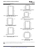
ADC0831-N, ADC0832-N, ADC0834-N, ADC0838-N www.ti.com SNAS531B – AUGUST 1999 – REVISED MARCH 2013 Timing Diagrams Figure 15. Data Input Timing Figure 16. Data Output Timing Figure 17. ADC0831-N Start Conversion Timing *LSB first output not available on ADC0831-N. Figure 18. ADC0831-N Timing Figure 19.
ADC0831-N, ADC0832-N, ADC0834-N, ADC0838-N SNAS531B – AUGUST 1999 – REVISED MARCH 2013 www.ti.com Figure 20.
ADC0831-N, ADC0832-N, ADC0834-N, ADC0838-N www.ti.com SNAS531B – AUGUST 1999 – REVISED MARCH 2013 *Make sure clock edge #18 clocks in the LSB before SE is taken low Figure 21.
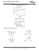
ADC0831-N, ADC0832-N, ADC0834-N, ADC0838-N SNAS531B – AUGUST 1999 – REVISED MARCH 2013 www.ti.com ADC0838-N Functional Block Diagram *Some of these functions/pins are not available with other options. Note 1: For the ADC0834-N, D1 is input directly to the D input of SELECT 1. SELECT 0 is forced to a “1”. For the ADC0832-N, DI is input directly to the DI input of ODD/SIGN. SELECT 0 is forced to a “0” and SELECT 1 is forced to a “1”.
ADC0831-N, ADC0832-N, ADC0834-N, ADC0838-N www.ti.com SNAS531B – AUGUST 1999 – REVISED MARCH 2013 Functional Description Multiplexer Addressing The design of these converters utilizes a sample-data comparator structure which provides for a differential analog input to be converted by a successive approximation routine. The actual voltage converted is always the difference between an assigned “+” input terminal and a “−” input terminal.
ADC0831-N, ADC0832-N, ADC0834-N, ADC0838-N SNAS531B – AUGUST 1999 – REVISED MARCH 2013 www.ti.com Table 3. MUX Addressing: ADC0838-N Differential MUX Mode MUX Address Analog Differential Channel-Pair # SGL/ ODD/ SELECT 0 DIF SIGN 1 0 0 1 0 0 0 0 + − 0 0 0 1 0 0 1 0 0 0 1 1 0 1 0 0 0 1 0 1 0 1 1 0 0 1 1 1 − 1 2 2 3 + − 3 4 5 + − 6 7 + − − + + − + − + Table 4.
ADC0831-N, ADC0832-N, ADC0834-N, ADC0838-N www.ti.com SNAS531B – AUGUST 1999 – REVISED MARCH 2013 THE DIGITAL INTERFACE A most important characteristic of these converters is their serial data link with the controlling processor.
ADC0831-N, ADC0832-N, ADC0834-N, ADC0838-N SNAS531B – AUGUST 1999 – REVISED MARCH 2013 www.ti.com 7. After 8 clock periods the conversion is completed. The SAR status line returns low to indicate this ½ clock cycle later. 8. If the programmer prefers, the data can be provided in an LSB first format [this makes use of the shift enable (SE) control line]. All 8 bits of the result are stored in an output shift register.
ADC0831-N, ADC0832-N, ADC0834-N, ADC0838-N www.ti.com SNAS531B – AUGUST 1999 – REVISED MARCH 2013 The Analog Inputs The most important feature of these converters is that they can be located right at the analog signal source and through just a few wires can communicate with a controlling processor with a highly noise immune serial bit stream. This in itself greatly minimizes circuitry to maintain analog signal accuracy which otherwise is most susceptible to noise pickup.
ADC0831-N, ADC0832-N, ADC0834-N, ADC0838-N SNAS531B – AUGUST 1999 – REVISED MARCH 2013 www.ti.com Adjusting for an Arbitrary Analog Input Voltage Range If the analog zero voltage of the A/D is shifted away from ground (for example, to accommodate an analog input signal which does not go to ground), this new zero reference should be properly adjusted first.
ADC0831-N, ADC0832-N, ADC0834-N, ADC0838-N www.ti.com SNAS531B – AUGUST 1999 – REVISED MARCH 2013 APPLICATIONS *4.5V ≤ VCC ≤ 6.3V Figure 25. Operating with a Temperature Compensated Reference Figure 26. Generating VCC from the Converter Clock *4.5V ≤ VCC ≤ 6.3V Figure 27. Using the A/D as the System Supply Regulator Figure 28. Remote Sensing— Clock and Power on 1 Wire Figure 29.
ADC0831-N, ADC0832-N, ADC0834-N, ADC0838-N SNAS531B – AUGUST 1999 – REVISED MARCH 2013 www.ti.
ADC0831-N, ADC0832-N, ADC0834-N, ADC0838-N www.ti.com SNAS531B – AUGUST 1999 – REVISED MARCH 2013 *Pinouts shown for ADC0838-N. For all other products tie to pin functions as shown. Figure 30. A “Stand-Alone” Hook-Up for ADC0838-N Evaluation Figure 31.
ADC0831-N, ADC0832-N, ADC0834-N, ADC0838-N SNAS531B – AUGUST 1999 – REVISED MARCH 2013 www.ti.com Figure 32. Digitizing a Current Flow *VIN(−) = 0.15 VCC 15% of VCC ≤ VXDR ≤ 85% of VCC Figure 33. Operating with Ratiometric Transducers Figure 34.
ADC0831-N, ADC0832-N, ADC0834-N, ADC0838-N www.ti.com SNAS531B – AUGUST 1999 – REVISED MARCH 2013 Figure 35. Zero-Shift and Span Adjust: 2V ≤ VIN ≤ 5V Figure 36. Obtaining Higher Resolution - 9-Bit A/D Controller performs a routine to determine which input polarity (9-bit example) or which channel pair (10-bit example) provides a non-zero output code. This information provides the extra bits. Figure 37.
ADC0831-N, ADC0832-N, ADC0834-N, ADC0838-N SNAS531B – AUGUST 1999 – REVISED MARCH 2013 www.ti.com Diodes are 1N914 Figure 38. Protecting the Input DO = all 1s if +VIN > −VIN DO = all 0s if +VIN < −VIN Figure 39.
ADC0831-N, ADC0832-N, ADC0834-N, ADC0838-N www.ti.com SNAS531B – AUGUST 1999 – REVISED MARCH 2013 •Uses one more wire than load cell itself •Two mini-DIPs could be mounted inside load cell for digital output transducer •Electronic offset and gain trims relax mechanical specs for gauge factor and offset •Low level cell output is converted immediately for high noise immunity Figure 40. Digital Load Cell •All power supplied by loop •1500V isolation at output Figure 41.
ADC0831-N, ADC0832-N, ADC0834-N, ADC0838-N SNAS531B – AUGUST 1999 – REVISED MARCH 2013 www.ti.com •No power required remotely •1500V isolation Figure 42.
ADC0831-N, ADC0832-N, ADC0834-N, ADC0838-N www.ti.com SNAS531B – AUGUST 1999 – REVISED MARCH 2013 Figure 43.
ADC0831-N, ADC0832-N, ADC0834-N, ADC0838-N SNAS531B – AUGUST 1999 – REVISED MARCH 2013 www.ti.com Figure 44.
ADC0831-N, ADC0832-N, ADC0834-N, ADC0838-N www.ti.com SNAS531B – AUGUST 1999 – REVISED MARCH 2013 REVISION HISTORY Changes from Revision A (March 2013) to Revision B • Page Changed layout of National Data Sheet to TI format ..........................................................................................................
PACKAGE OPTION ADDENDUM www.ti.
PACKAGE OPTION ADDENDUM www.ti.
PACKAGE OPTION ADDENDUM www.ti.com 1-Nov-2013 (6) Lead/Ball Finish - Orderable Devices may have multiple material finish options. Finish options are separated by a vertical ruled line. Lead/Ball Finish values may wrap to two lines if the finish value exceeds the maximum column width. Important Information and Disclaimer:The information provided on this page represents TI's knowledge and belief as of the date that it is provided.
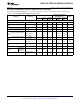
PACKAGE MATERIALS INFORMATION www.ti.com 23-Sep-2013 TAPE AND REEL INFORMATION *All dimensions are nominal Device Package Package Pins Type Drawing SPQ Reel Reel A0 Diameter Width (mm) (mm) W1 (mm) B0 (mm) K0 (mm) P1 (mm) W Pin1 (mm) Quadrant ADC0831CCWMX/NOPB SOIC NPA 14 1000 330.0 16.4 10.9 9.5 3.2 12.0 16.0 Q1 ADC0832CCWMX SOIC NPA 14 1000 330.0 16.4 10.9 9.5 3.2 12.0 16.0 Q1 ADC0832CCWMX/NOPB SOIC NPA 14 1000 330.0 16.4 10.9 9.5 3.2 12.0 16.
PACKAGE MATERIALS INFORMATION www.ti.com 23-Sep-2013 *All dimensions are nominal Device Package Type Package Drawing Pins SPQ Length (mm) Width (mm) Height (mm) ADC0831CCWMX/NOPB SOIC NPA 14 1000 367.0 367.0 38.0 ADC0832CCWMX SOIC NPA 14 1000 367.0 367.0 38.0 ADC0832CCWMX/NOPB SOIC NPA 14 1000 367.0 367.0 38.0 ADC0834CCWMX/NOPB SOIC NPA 14 1000 367.0 367.0 38.0 ADC0838CCWMX SOIC DW 20 1000 367.0 367.0 45.0 ADC0838CCWMX/NOPB SOIC DW 20 1000 367.0 367.
MECHANICAL DATA NFF0014A N0014A N14A (Rev G) www.ti.
MECHANICAL DATA NFH0020A N0020A N20A (Rev G) www.ti.
MECHANICAL DATA NPA0014B www.ti.
IMPORTANT NOTICE Texas Instruments Incorporated and its subsidiaries (TI) reserve the right to make corrections, enhancements, improvements and other changes to its semiconductor products and services per JESD46, latest issue, and to discontinue any product or service per JESD48, latest issue. Buyers should obtain the latest relevant information before placing orders and should verify that such information is current and complete.