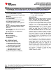
ADC12030, ADC12032, ADC12034 ADC12038, ADC12H030, ADC12H032 ADC12H034, ADC12H038 www.ti.
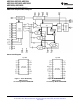
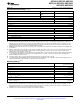
ADC12030, ADC12032, ADC12034 ADC12038, ADC12H030, ADC12H032 ADC12H034, ADC12H038 SNAS080K – JULY 1999 – REVISED MARCH 2013 www.ti.com ADC12038 Simplified Block Diagram Connection Diagram Top View Figure 1. 16-Pin Wide Body SOIC Package See Package Number DW0016B 2 Submit Documentation Feedback Top View Figure 2.
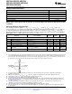
ADC12030, ADC12032, ADC12034 ADC12038, ADC12H030, ADC12H032 ADC12H034, ADC12H038 www.ti.com SNAS080K – JULY 1999 – REVISED MARCH 2013 Top View Top View Figure 3. 24-Pin Wide Body SOIC, PDIP, SSOP Packages See Package Numbers DW0024B, NAM0024D, DB0024A Figure 4. 28-Pin Wide Body SOIC Package See Package Number DW0028B PIN DESCRIPTIONS Pin Name CH0 thru CH7 COM Pin Description Analog Inputs to the MUX (multiplexer).
ADC12030, ADC12032, ADC12034 ADC12038, ADC12H030, ADC12H032 ADC12H034, ADC12H038 SNAS080K – JULY 1999 – REVISED MARCH 2013 www.ti.com PIN DESCRIPTIONS (continued) Pin Name Pin Description CS Chip Select input pin. When a logic low is applied to this pin, the rising edge of SCLK shifts the data on DI into the address register. This low also brings DO out of TRI-STATE.
ADC12030, ADC12032, ADC12034 ADC12038, ADC12H030, ADC12H032 ADC12H034, ADC12H038 www.ti.com SNAS080K – JULY 1999 – REVISED MARCH 2013 Absolute Maximum Ratings (1) (2) (3) Positive Supply Voltage (V+ = VA+ = VD+) Voltage at Inputs and Outputs except CH0–CH7 and COM Voltage at Analog Inputs CH0–CH7 and COM 6.5V + −0.3V to (V +0.
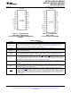
ADC12030, ADC12032, ADC12034 ADC12038, ADC12H030, ADC12H032 ADC12H034, ADC12H038 SNAS080K – JULY 1999 – REVISED MARCH 2013 www.ti.com Package Thermal Resistance Part Number Thermal Resistance (θJA) ADC12(H)030CIWM 70°C/W ADC12032CIWM 64°C/W ADC12034CIN 42°C/W ADC12034CIWM 57°C/W ADC12H034CIMSA 97°C/W ADC12(H)038CIWM 50°C/W NOTE: Some of these devices may be obsolete or on Lifetime Buy status. Check our web site for product availability.
ADC12030, ADC12032, ADC12034 ADC12038, ADC12H030, ADC12H032 ADC12H034, ADC12H038 www.ti.com SNAS080K – JULY 1999 – REVISED MARCH 2013 Converter Electrical Characteristics (continued) The following specifications apply for V+ = VA+ = VD+ = +5.0 VDC, VREF+ = +4.
ADC12030, ADC12032, ADC12034 ADC12038, ADC12H030, ADC12H032 ADC12H034, ADC12H038 SNAS080K – JULY 1999 – REVISED MARCH 2013 www.ti.com Converter Electrical Characteristics (continued) The following specifications apply for V+ = VA+ = VD+ = +5.0 VDC, VREF+ = +4.
ADC12030, ADC12032, ADC12034 ADC12038, ADC12H030, ADC12H032 ADC12H034, ADC12H038 www.ti.com SNAS080K – JULY 1999 – REVISED MARCH 2013 DC and Logic Electrical Characteristics (continued) The following specifications apply for V+ = VA+ = VD+ = +5.0 VDC, VREF+ = +4.
ADC12030, ADC12032, ADC12034 ADC12038, ADC12H030, ADC12H032 ADC12H034, ADC12H038 SNAS080K – JULY 1999 – REVISED MARCH 2013 www.ti.com AC Electrical Characteristics (continued) The following specifications apply for V+ = VA+ = VD+ = +5.0 VDC, VREF+ = +4.
ADC12030, ADC12032, ADC12034 ADC12038, ADC12H030, ADC12H032 ADC12H034, ADC12H038 www.ti.com SNAS080K – JULY 1999 – REVISED MARCH 2013 Timing Characteristics The following specifications apply for V+ = VA+ = VD+ = +5.0 VDC, VREF+ = +4.
ADC12030, ADC12032, ADC12034 ADC12038, ADC12H030, ADC12H032 ADC12H034, ADC12H038 SNAS080K – JULY 1999 – REVISED MARCH 2013 www.ti.com Figure 5. Transfer Characteristic Figure 6. Simplified Error Curve vs.
ADC12030, ADC12032, ADC12034 ADC12038, ADC12H030, ADC12H032 ADC12H034, ADC12H038 www.ti.com SNAS080K – JULY 1999 – REVISED MARCH 2013 Figure 7. Simplified Error Curve vs. Output Code after Auto Calibration Cycle Figure 8.
ADC12030, ADC12032, ADC12034 ADC12038, ADC12H030, ADC12H032 ADC12H034, ADC12H038 SNAS080K – JULY 1999 – REVISED MARCH 2013 www.ti.com Typical Performance Characteristics (1) The following curves apply for 12-bit + sign mode after Auto Calibration unless otherwise specified. The performance for 8-bit + sign mode is equal to or better than shown. (1) 14 Linearity Error Change vs. Clock Frequency Linearity Error Change vs. Temperature Figure 9. Figure 10. Linearity Error Change vs.
ADC12030, ADC12032, ADC12034 ADC12038, ADC12H030, ADC12H032 ADC12H034, ADC12H038 www.ti.com SNAS080K – JULY 1999 – REVISED MARCH 2013 Typical Performance Characteristics (1) (continued) The following curves apply for 12-bit + sign mode after Auto Calibration unless otherwise specified. The performance for 8-bit + sign mode is equal to or better than shown. Full-Scale Error Change vs. Reference Voltage Full-Scale Error Change vs. Supply Voltage Figure 15. Figure 16. Offset or Zero Error Change vs.
ADC12030, ADC12032, ADC12034 ADC12038, ADC12H030, ADC12H032 ADC12H034, ADC12H038 SNAS080K – JULY 1999 – REVISED MARCH 2013 www.ti.com Typical Performance Characteristics (1) (continued) The following curves apply for 12-bit + sign mode after Auto Calibration unless otherwise specified. The performance for 8-bit + sign mode is equal to or better than shown. Analog Supply Current vs. Temperature Digital Supply Current vs. Clock Frequency Figure 21. Figure 22. Digital Supply Current vs.
ADC12030, ADC12032, ADC12034 ADC12038, ADC12H030, ADC12H032 ADC12H034, ADC12H038 www.ti.com SNAS080K – JULY 1999 – REVISED MARCH 2013 Typical Dynamic Performance Characteristics The following curves apply for 12-bit + sign mode after Auto Calibration unless otherwise specified. Bipolar Spectral Response with 1 kHz Sine Wave Input Bipolar Spectral Response with 10 kHz Sine Wave Input Figure 24. Figure 25.
ADC12030, ADC12032, ADC12034 ADC12038, ADC12H030, ADC12H032 ADC12H034, ADC12H038 SNAS080K – JULY 1999 – REVISED MARCH 2013 www.ti.com Typical Dynamic Performance Characteristics (continued) The following curves apply for 12-bit + sign mode after Auto Calibration unless otherwise specified. 18 Bipolar Spurious Free Dynamic Range Unipolar Signal-to-Noise Ratio vs. Input Frequency Figure 30. Figure 31. Unipolar Signal-to-Noise + Distortion Ratio vs.
ADC12030, ADC12032, ADC12034 ADC12038, ADC12H030, ADC12H032 ADC12H034, ADC12H038 www.ti.com SNAS080K – JULY 1999 – REVISED MARCH 2013 Typical Dynamic Performance Characteristics (continued) The following curves apply for 12-bit + sign mode after Auto Calibration unless otherwise specified. Unipolar Spectral Response with 20 kHz Sine Wave Input Unipolar Spectral Response with 30 kHz Sine Wave Input Figure 36. Figure 37.
ADC12030, ADC12032, ADC12034 ADC12038, ADC12H030, ADC12H032 ADC12H034, ADC12H038 SNAS080K – JULY 1999 – REVISED MARCH 2013 www.ti.com Test Circuits Figure 40. DO “TRI-STATE” (t1H, tOH) Figure 41. DO except “TRI-STATE” Figure 42. Leakage Current Timing Diagrams Figure 43. DO Falling and Rising Edge Figure 44.
ADC12030, ADC12032, ADC12034 ADC12038, ADC12H030, ADC12H032 ADC12H034, ADC12H038 www.ti.com SNAS080K – JULY 1999 – REVISED MARCH 2013 Figure 45. DI Data Input Timing Figure 46. DO Data Output Timing Using CS 0 1 2 3 4 n SCLK tSET-UP CS tDDO tHDO tHDO tACC DO 2.4V 2.4V 0.4V tDDO 0.4V 2.4V tSD tCD DOR EOC Figure 47.
ADC12030, ADC12032, ADC12034 ADC12038, ADC12H030, ADC12H032 ADC12H034, ADC12H038 SNAS080K – JULY 1999 – REVISED MARCH 2013 www.ti.com Note: DO output data is not valid during this cycle. Figure 48. ADC12038 Auto Cal or Auto Zero Figure 49.
ADC12030, ADC12032, ADC12034 ADC12038, ADC12H030, ADC12H032 ADC12H034, ADC12H038 www.ti.com SNAS080K – JULY 1999 – REVISED MARCH 2013 Figure 50. ADC12038 Read Data without Starting a Conversion with CS Continuously Low Figure 51.
ADC12030, ADC12032, ADC12034 ADC12038, ADC12H030, ADC12H032 ADC12H034, ADC12H038 SNAS080K – JULY 1999 – REVISED MARCH 2013 www.ti.com Figure 52. ADC12038 Conversion Using CS with 16-Bit Digital Output Format Figure 53.
ADC12030, ADC12032, ADC12034 ADC12038, ADC12H030, ADC12H032 ADC12H034, ADC12H038 www.ti.com SNAS080K – JULY 1999 – REVISED MARCH 2013 Figure 54. ADC12038 Conversion with CS Continuously Low and 16-Bit Digital Output Format Figure 55.
ADC12030, ADC12032, ADC12034 ADC12038, ADC12H030, ADC12H032 ADC12H034, ADC12H038 SNAS080K – JULY 1999 – REVISED MARCH 2013 www.ti.com Figure 56. ADC12038 Software Power Up/Down with CS Continuously Low and 16-Bit Digital Output Format Note: Hardware power up/down may occur at any time. If PD is high while a conversion is in progress that conversion will be corrupted and erroneous data will be stored in the output shift register. Figure 57.
ADC12030, ADC12032, ADC12034 ADC12038, ADC12H030, ADC12H032 ADC12H034, ADC12H038 www.ti.com SNAS080K – JULY 1999 – REVISED MARCH 2013 Note: In order for all 9 bits of Status Information to be accessible, the last conversion programmed before Cycle N needs to have a resolution of 8 bits plus sign, 12 bits, 12 bits plus sign, or greater. Figure 58. ADC12038 Configuration Modification—Example of a Status Read VA+ ANALOG INPUT VOLTAGE ASSIGNED (+) INPUT VD+ ** 0.01 uF ** 0.1 uF 10 uF * ** 0.
ADC12030, ADC12032, ADC12034 ADC12038, ADC12H030, ADC12H032 ADC12H034, ADC12H038 SNAS080K – JULY 1999 – REVISED MARCH 2013 www.ti.com Format and Set-Up Tables Table 1.
ADC12030, ADC12032, ADC12034 ADC12038, ADC12H030, ADC12H032 ADC12H034, ADC12H038 www.ti.com SNAS080K – JULY 1999 – REVISED MARCH 2013 Table 3.
ADC12030, ADC12032, ADC12034 ADC12038, ADC12H030, ADC12H032 ADC12H034, ADC12H038 SNAS080K – JULY 1999 – REVISED MARCH 2013 www.ti.com Table 5.
ADC12030, ADC12032, ADC12034 ADC12038, ADC12H030, ADC12H032 ADC12H034, ADC12H038 www.ti.com SNAS080K – JULY 1999 – REVISED MARCH 2013 APPLICATIONS INFORMATION 1.0 DIGITAL INTERFACE 1.1 Interface Concepts The example in Figure 61 shows a typical sequence of events after the power is applied to the ADC12030/2/4/8: Figure 61. Typical Power Supply Power Up Sequence The first instruction input to the ADC via DI initiates Auto Cal. The data output on DO at that time is meaningless and is completely random.
ADC12030, ADC12032, ADC12034 ADC12038, ADC12H030, ADC12H032 ADC12H034, ADC12H038 SNAS080K – JULY 1999 – REVISED MARCH 2013 www.ti.com 1.3 CS Low Continuously Considerations When CS is continuously low, it is important to transmit the exact number of SCLK pulses that the ADC expects. Not doing so will desynchronize the serial communications to the ADC. When the supply power is first applied to the ADC, it will expect to see 13 SCLK pulses for each I/O transmission.
ADC12030, ADC12032, ADC12034 ADC12038, ADC12H030, ADC12H032 ADC12H034, ADC12H038 www.ti.com SNAS080K – JULY 1999 – REVISED MARCH 2013 Hardware power up/down is controlled by the state of the PD pin. Software power-up/down is controlled by the instruction issued to the ADC. If a software power up instruction is issued to the ADC while a hardware power down is in effect (PD pin high) the device will remain in the power-down state.
ADC12030, ADC12032, ADC12034 ADC12038, ADC12H030, ADC12H032 ADC12H034, ADC12H038 SNAS080K – JULY 1999 – REVISED MARCH 2013 www.ti.com 1.8 Brown Out Conditions When the supply voltage dips below about 2.7V, the internal registers, including the calibration coefficients and all of the other registers, may lose their contents. When this happens the ADC will not perform as expected or not at all after power is fully restored.
ADC12030, ADC12032, ADC12034 ADC12038, ADC12H030, ADC12H032 ADC12H034, ADC12H038 www.ti.com SNAS080K – JULY 1999 – REVISED MARCH 2013 2.1 Biasing for Various Multiplexer Configurations Figure 65 is an example of device connections for single-ended operation. The sign bit is always low. The digital output range is 0 0000 0000 0000 to 0 1111 1111 1111. One LSB is equal to 1 mV (4.1V/4096 LSBs). ANALOG INPUT VOLTAGE RANGE 0V TO 4.096V 12-BITS UNSIGNED ASSIGNED (+) INPUT CH0 CH2 CH4 or CH6 VA+ 0.
ADC12030, ADC12032, ADC12034 ADC12038, ADC12H030, ADC12H032 ADC12H034, ADC12H038 SNAS080K – JULY 1999 – REVISED MARCH 2013 www.ti.com In the circuit of Figure 67, some voltage range is lost since the amplifier will not be able to swing to +5V and GND with a single +5V supply. Using an adjustable version of the LM4041 to set the full scale voltage at exactly 2.048V and a lower grade LM4040D-2.5 to bias up everything to 2.
ADC12030, ADC12032, ADC12034 ADC12038, ADC12H030, ADC12H032 ADC12H034, ADC12H038 www.ti.com SNAS080K – JULY 1999 – REVISED MARCH 2013 ANALOG INPUT VOLTAGE RANGE 0.45V to 4.55V ASSIGNED (+) INPUT CH0 CH2 CH4 or CH6 FULLY DIFFERENTIAL 12-BIT PLUS SIGN ANALOG INPUT VOLTAGE RANGE 0.45V to 4.55V VA+ 0.01 uF 0.1 uF 10 uF VD+ 0.01 uF 0.1 uF 10 uF +5.0V 1k ADC1203Y ASSIGNED (-) INPUT CH1 CH3 CH5 or CH7 VREF+ +4.1V 0.01 uF 0.1 uF 10 uF LM4040-4.
ADC12030, ADC12032, ADC12034 ADC12038, ADC12H030, ADC12H032 ADC12H034, ADC12H038 SNAS080K – JULY 1999 – REVISED MARCH 2013 www.ti.com Part Number Output Voltage Tolerance Temperature Coefficient LM4041CI-Adj ±0.5% ±100ppm/°C LM4040AI-4.1 ±0.1% ±100ppm/°C LM4120AI-4.1 ±0.2% ±50ppm/°C LM4121AI-4.1 ±0.2% ±50ppm/°C LM4050AI-4.1 ±0.1% ±50ppm/°C LM4030AI-4.1 ±0.05% ±10ppm/°C ±0.1% ±3.0ppm/°C LM4140AC-4.
ADC12030, ADC12032, ADC12034 ADC12038, ADC12H030, ADC12H032 ADC12H034, ADC12H038 www.ti.com SNAS080K – JULY 1999 – REVISED MARCH 2013 for (8-bit) resolution the Output Code = (2) Round off to the nearest integer value between −4096 to 4095 for 12-bit resolution and between −256 to 255 for 8-bit resolution if the result of the above equation is not a whole number. Examples are shown in the table below: VREF+ VREF− VIN+ VIN− Digital Output Code +2.5V +1V +1.5V 0V 0,1111,1111,1111 +4.
ADC12030, ADC12032, ADC12034 ADC12038, ADC12H030, ADC12H032 ADC12H034, ADC12H038 SNAS080K – JULY 1999 – REVISED MARCH 2013 www.ti.com 9.0 POWER SUPPLIES Noise spikes on the VA+ and VD+ supply lines can cause conversion errors; the comparator will respond to the noise. The ADC is especially sensitive to any power supply spikes that occur during the Auto Zero or linearity correction.
ADC12030, ADC12032, ADC12034 ADC12038, ADC12H030, ADC12H032 ADC12H034, ADC12H038 www.ti.com SNAS080K – JULY 1999 – REVISED MARCH 2013 where • "n" is the ADC's resolution in bits (4) The effective bits of an actual ADC is found to be: n(effective) = ENOB = (S/(N + D) - 1.76 / 6.02 (5) As an example, this device with a differential signed 5V, 1 kHz sine wave input signal will typically have a S/(N + D) of 77 dB, which is equivalent to 12.5 effective bits. 15.
ADC12030, ADC12032, ADC12034 ADC12038, ADC12H030, ADC12H032 ADC12H034, ADC12H038 SNAS080K – JULY 1999 – REVISED MARCH 2013 www.ti.com The ADC powers up with No Auto Cal, No Auto Zero, 10 CCLK Acquisition Time, 12-bit conversion, data out with sign, power up, 12- or 13-bit MSB first, and user mode. Auto Cal, Auto Zero, Power Up and Power Down instructions do not change these default settings. The following power up sequence should be followed: 1. Run the program 2.
ADC12030, ADC12032, ADC12034 ADC12038, ADC12H030, ADC12H032 ADC12H034, ADC12H038 www.ti.
ADC12030, ADC12032, ADC12034 ADC12038, ADC12H030, ADC12H032 ADC12H034, ADC12H038 SNAS080K – JULY 1999 – REVISED MARCH 2013 www.ti.com REVISION HISTORY Changes from Revision J (March 2013) to Revision K • 44 Page Changed layout of National Data Sheet to TI format ..........................................................................................................
PACKAGE OPTION ADDENDUM www.ti.
PACKAGE OPTION ADDENDUM www.ti.com 1-Nov-2013 (5) Multiple Device Markings will be inside parentheses. Only one Device Marking contained in parentheses and separated by a "~" will appear on a device. If a line is indented then it is a continuation of the previous line and the two combined represent the entire Device Marking for that device. (6) Lead/Ball Finish - Orderable Devices may have multiple material finish options. Finish options are separated by a vertical ruled line.
PACKAGE MATERIALS INFORMATION www.ti.com 23-Sep-2013 TAPE AND REEL INFORMATION *All dimensions are nominal Device ADC12030CIWMX/NOPB Package Package Pins Type Drawing SPQ Reel Reel A0 Diameter Width (mm) (mm) W1 (mm) B0 (mm) K0 (mm) P1 (mm) W Pin1 (mm) Quadrant SOIC DW 16 1000 330.0 16.4 10.9 10.7 3.2 12.0 16.0 Q1 ADC12038CIWMX/NOPB SOIC DW 28 1000 330.0 24.4 10.8 18.4 3.2 12.0 24.0 Q1 ADC12H034CIMSAX/NOP B SSOP DB 24 2000 330.0 16.4 8.6 8.9 2.5 12.0 16.
PACKAGE MATERIALS INFORMATION www.ti.com 23-Sep-2013 *All dimensions are nominal Device Package Type Package Drawing Pins SPQ Length (mm) Width (mm) Height (mm) ADC12030CIWMX/NOPB SOIC DW 16 1000 367.0 367.0 38.0 ADC12038CIWMX/NOPB SOIC DW 28 1000 367.0 367.0 45.0 ADC12H034CIMSAX/NOP B SSOP DB 24 2000 367.0 367.0 38.
MECHANICAL DATA MSSO002E – JANUARY 1995 – REVISED DECEMBER 2001 DB (R-PDSO-G**) PLASTIC SMALL-OUTLINE 28 PINS SHOWN 0,38 0,22 0,65 28 0,15 M 15 0,25 0,09 8,20 7,40 5,60 5,00 Gage Plane 1 14 0,25 A 0°–ā8° 0,95 0,55 Seating Plane 2,00 MAX 0,10 0,05 MIN PINS ** 14 16 20 24 28 30 38 A MAX 6,50 6,50 7,50 8,50 10,50 10,50 12,90 A MIN 5,90 5,90 6,90 7,90 9,90 9,90 12,30 DIM 4040065 /E 12/01 NOTES: A. B. C. D. All linear dimensions are in millimeters.
IMPORTANT NOTICE Texas Instruments Incorporated and its subsidiaries (TI) reserve the right to make corrections, enhancements, improvements and other changes to its semiconductor products and services per JESD46, latest issue, and to discontinue any product or service per JESD48, latest issue. Buyers should obtain the latest relevant information before placing orders and should verify that such information is current and complete.