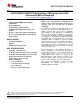
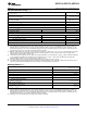
ADC12130, ADC12132, ADC12138 www.ti.com SNAS098G – MARCH 2000 – REVISED MARCH 2013 ADC12130/ADC12132/ADC12138 Self-Calibrating 12-Bit Plus Sign Serial I/O A/D Converters with MUX and Sample/Hold Check for Samples: ADC12130, ADC12132, ADC12138 FEATURES DESCRIPTION • NOTE: Some device/package combinations are obsolete and are described and shown here for reference only. See our web site for product availability.
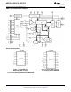
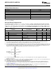
ADC12130, ADC12132, ADC12138 SNAS098G – MARCH 2000 – REVISED MARCH 2013 www.ti.com ADC12138 Simplified Block Diagram Connection Diagrams Top View Figure 1. 16-Pin MDIP and Wide Body SOIC Packages See Package Number NFG0016E and DW0016B 2 Submit Documentation Feedback Top View Figure 2.
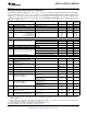
ADC12130, ADC12132, ADC12138 www.ti.com SNAS098G – MARCH 2000 – REVISED MARCH 2013 Top View Figure 3. 28-Pin MDIP, SSOP and Wide Body SOIC Packages See Package Numbers N28B, DB0028A, and DW0028B Some of these product/package combinations are obsolete and are shown here for reference only. Check the TI web site for availability. PIN DESCRIPTIONS Pin Name CH0 thru CH7 COM MUXOUT1 MUXOUT2 Pin Description Analog Inputs to the MUX (multiplexer).
ADC12130, ADC12132, ADC12138 SNAS098G – MARCH 2000 – REVISED MARCH 2013 www.ti.com PIN DESCRIPTIONS (continued) Pin Name Pin Description CS Chip Select input pin. When a logic low is applied to this pin, the rising edge of SCLK shifts the data at the DI input into the address register and brings DO out of TRI-STATE. With CS low, the falling edge of SCLK shifts the data resulting from the previous ADC conversion out at the DO output, with the exception of the first bit of data.
ADC12130, ADC12132, ADC12138 www.ti.com SNAS098G – MARCH 2000 – REVISED MARCH 2013 Absolute Maximum Ratings (1) (2) Positive Supply Voltage (V+ = VA+ = VD+) 6.5V Voltage at Inputs and Outputs except CH0–CH7 and COM −0.3V to V+ +0.
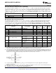
ADC12130, ADC12132, ADC12138 SNAS098G – MARCH 2000 – REVISED MARCH 2013 www.ti.com Package Thermal Resistance Part Number Thermal Resistance (θJA) ADC12130CIN 53°C/W ADC12130CIWM 70°C/W ADC12132CIMSA 134°C/W ADC12132CIWM 64°C/W ADC121038CIN 40°C/W ADC121038CIMSA 97°C/W ADC12138CIWM 50°C/W Some of these product/package combinations are obsolete and are shown here for reference only. Check the TI web site for availability.
ADC12130, ADC12132, ADC12138 www.ti.com SNAS098G – MARCH 2000 – REVISED MARCH 2013 Converter Electrical Characteristics (continued) The following specifications apply for (V+ = VA+ = VD+ = +5V, VREF+ = +4.096V, and fully differential input with fixed 2.048V common-mode voltage) or (V+ = VA+ = VD+ = 3.3V, VREF+ = 2.5V and fully-differential input with fixed 1.
ADC12130, ADC12132, ADC12138 SNAS098G – MARCH 2000 – REVISED MARCH 2013 www.ti.com Converter Electrical Characteristics (continued) The following specifications apply for (V+ = VA+ = VD+ = +5V, VREF+ = +4.096V, and fully differential input with fixed 2.048V common-mode voltage) or (V+ = VA+ = VD+ = 3.3V, VREF+ = 2.5V and fully-differential input with fixed 1.
ADC12130, ADC12132, ADC12138 www.ti.com SNAS098G – MARCH 2000 – REVISED MARCH 2013 DC and Logic Electrical Characteristics (continued) The following specifications apply for (V+ = VA+ = VD+ = +5V, VREF+ = +4.096V, and fully-differential input with fixed 2.048V common-mode voltage) or (V+ = VA+ = VD+ = +3.3V, VREF+ = +2.5V and fully-differential input with fixed 1.
ADC12130, ADC12132, ADC12138 SNAS098G – MARCH 2000 – REVISED MARCH 2013 www.ti.com AC Electrical Characteristics (continued) The following specifications apply for (V+ = VA+ = VD+ = +5V, VREF+ = +4.096V, and fully-differential input with fixed 2.048V common-mode voltage) or (V+ = VA+ = VD+ = +3.3V, VREF+ = +2.5V and fully-differential input with fixed 1.
ADC12130, ADC12132, ADC12138 www.ti.com SNAS098G – MARCH 2000 – REVISED MARCH 2013 AC Electrical Characteristics (continued) The following specifications apply for (V+ = VA+ = VD+ = +5V, VREF+ = +4.096V, and fully-differential input with fixed 2.048V common-mode voltage) or (V+ = VA+ = VD+ = +3.3V, VREF+ = +2.5V and fully-differential input with fixed 1.
ADC12130, ADC12132, ADC12138 SNAS098G – MARCH 2000 – REVISED MARCH 2013 www.ti.com Figure 4. Transfer Characteristic Figure 5. Simplified Error Curve vs.
ADC12130, ADC12132, ADC12138 www.ti.com SNAS098G – MARCH 2000 – REVISED MARCH 2013 Figure 6. Simplified Error Curve vs. Output Code after Auto Calibration Cycle Figure 7.
ADC12130, ADC12132, ADC12138 SNAS098G – MARCH 2000 – REVISED MARCH 2013 www.ti.com Typical Performance Characteristics The following curves apply for 12-bit + sign mode after Auto Calibration unless otherwise specified. 14 Linearity Error Change vs. Clock Frequency Linearity Error Change vs. Temperature Figure 8. Figure 9. Linearity Error Change vs. Reference Voltage Linearity Error Change vs. Supply Voltage Figure 10. Figure 11. Full-Scale Error Change vs.
ADC12130, ADC12132, ADC12138 www.ti.com SNAS098G – MARCH 2000 – REVISED MARCH 2013 Typical Performance Characteristics (continued) The following curves apply for 12-bit + sign mode after Auto Calibration unless otherwise specified. Full-Scale Error Change vs. Reference Voltage Full-Scale Error Change vs. Supply Voltage Figure 14. Figure 15. Offset or Zero Error Change vs. Clock Frequency Offset or Zero Error Change vs. Temperature Figure 16. Figure 17. Offset or Zero Error Change vs.
ADC12130, ADC12132, ADC12138 SNAS098G – MARCH 2000 – REVISED MARCH 2013 www.ti.com Typical Performance Characteristics (continued) The following curves apply for 12-bit + sign mode after Auto Calibration unless otherwise specified. 16 Analog Supply Current vs. Temperature Digital Supply Current vs. Clock Frequency Figure 20. Figure 21. Digital Supply Current vs. Temperature Linearity Error Change vs. Temperature Figure 22. Figure 23. Full-Scale Error Change vs.
ADC12130, ADC12132, ADC12138 www.ti.com SNAS098G – MARCH 2000 – REVISED MARCH 2013 Typical Performance Characteristics (continued) The following curves apply for 12-bit + sign mode after Auto Calibration unless otherwise specified. Offset or Zero Error Change vs. Temperature Offset or Zero Error Change vs. Supply Voltage Figure 26. Figure 27. Analog Supply Current vs. Temperature Digital Supply Current vs. Temperature Figure 28. Figure 29.
ADC12130, ADC12132, ADC12138 SNAS098G – MARCH 2000 – REVISED MARCH 2013 www.ti.com Typical Dynamic Performance Characteristics The following curves apply for 12-bit + sign mode after Auto Calibration unless otherwise specified. 18 Bipolar Spectral Response with 1 kHz Sine Wave Input Bipolar Spectral Response with 10 kHz Sine Wave Input Figure 30. Figure 31. Bipolar Spectral Response with 20 kHz Sine Wave Input Bipolar Spectral Response with 30 kHz Sine Wave Input Figure 32. Figure 33.
ADC12130, ADC12132, ADC12138 www.ti.com SNAS098G – MARCH 2000 – REVISED MARCH 2013 Typical Dynamic Performance Characteristics (continued) The following curves apply for 12-bit + sign mode after Auto Calibration unless otherwise specified. Bipolar Spurious Free Dynamic Range Unipolar Signal-to-Noise Ratio vs. Input Frequency Figure 36. Figure 37. Unipolar Signal-to-Noise + Distortion Ratio vs. Input Frequency Unipolar Signal-to-Noise + Distortion Ratio vs. Input Signal Level Figure 38. Figure 39.
ADC12130, ADC12132, ADC12138 SNAS098G – MARCH 2000 – REVISED MARCH 2013 www.ti.com Typical Dynamic Performance Characteristics (continued) The following curves apply for 12-bit + sign mode after Auto Calibration unless otherwise specified. 20 Unipolar Spectral Response with 20 kHz Sine Wave Input Unipolar Spectral Response with 30 kHz Sine Wave Input Figure 42. Figure 43. Unipolar Spectral Response with 40 kHz Sine Wave Input Unipolar Spectral Response with 50 kHz Sine Wave Input Figure 44.
ADC12130, ADC12132, ADC12138 www.ti.com SNAS098G – MARCH 2000 – REVISED MARCH 2013 Test Circuits Figure 46. DO “TRI-STATE” (t1H, t0H) Figure 47. DO except “TRI-STATE” Figure 48. Leakage Current Timing Diagrams Figure 49. DO Falling and Rising Edge Figure 50.
ADC12130, ADC12132, ADC12138 SNAS098G – MARCH 2000 – REVISED MARCH 2013 www.ti.com Figure 51. DI Data Input Timing Figure 52. DO Data Output Timing Using CS 0 1 2 3 4 n SCLK tSET-UP CS tDDO tHDO tHDO tACC DO 2.4V 2.4V 0.4V tDDO 0.4V 2.4V tSD tCD DOR EOC Figure 53.
ADC12130, ADC12132, ADC12138 www.ti.com SNAS098G – MARCH 2000 – REVISED MARCH 2013 Note: DO output data is not valid during this cycle. Figure 54. ADC12138 Auto Cal or Auto Zero Figure 55.
ADC12130, ADC12132, ADC12138 SNAS098G – MARCH 2000 – REVISED MARCH 2013 www.ti.com Figure 56. ADC12138 Read Data without Starting a Conversion with CS Continuously Low Figure 57.
ADC12130, ADC12132, ADC12138 www.ti.com SNAS098G – MARCH 2000 – REVISED MARCH 2013 Figure 58. ADC12138 Conversion with CS Continuously Low and 16-Bit Digital Output Format Figure 59.
ADC12130, ADC12132, ADC12138 SNAS098G – MARCH 2000 – REVISED MARCH 2013 www.ti.com Figure 60. ADC12138 Software Power Up/Down with CS Continuously Low and 16-Bit Digital Output Format Note: Hardware power up/down may occur at any time. If PD is high while a conversion is in progress that conversion will be corrupted and erroneous data will be stored in the output shift register. Figure 61.
ADC12130, ADC12132, ADC12138 www.ti.com SNAS098G – MARCH 2000 – REVISED MARCH 2013 Figure 62. ADC12138 Configuration Modification—Example of a Status Read VA+ ANALOG INPUT VOLTAGE ASSIGNED (+) INPUT VD+ ** 0.01 uF ** 0.1 uF 10 uF * ** 0.01 uF ** 0.1 uF 10 uF * ** 0.01 uF ** 0.1 uF 10 uF * +5.0V ADC ANALOG INPUT VOLTAGE ASSIGNED (-) INPUT VREF+ +4.096V VREFAGND DGND ANALOG INPUT VOLTAGE GROUND REFERENCE *Tantalum **Monolithic Ceramic or better Figure 63.
ADC12130, ADC12132, ADC12138 SNAS098G – MARCH 2000 – REVISED MARCH 2013 www.ti.com Format and Set-Up Tables Table 1.
ADC12130, ADC12132, ADC12138 www.ti.com SNAS098G – MARCH 2000 – REVISED MARCH 2013 Table 3.
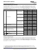
ADC12130, ADC12132, ADC12138 SNAS098G – MARCH 2000 – REVISED MARCH 2013 www.ti.com Table 6. Status Register Status Bit Location Status Bit DB0 PU DB1 DB2 PD Cal DB3 DB4 12 or 13 Device Status Function 30 “High” indicates a Power Up Sequence is in progress “High” indicates a Power Down Sequence is in progress Submit Documentation Feedback DB5 DB6 DB7 DB8 16 or 17 Sign Justification Test Mode When “High” the conversion result will be output MSB first.
ADC12130, ADC12132, ADC12138 www.ti.com SNAS098G – MARCH 2000 – REVISED MARCH 2013 APPLICATION INFORMATION NOTE: Some of the device/package combinations are obsolete and are shown and described here for reference only. Please see the TI web site for availability. 1.0 DIGITAL INTERFACE 1.1 Interface Concepts The example in Figure 65 shows a typical sequence of events after the power is applied to the ADC12130/2/8: Figure 65.
ADC12130, ADC12132, ADC12138 SNAS098G – MARCH 2000 – REVISED MARCH 2013 www.ti.com 1.3 CS Low Continuously Considerations When CS is continuously low, it is important to transmit the exact number of SCLK pulses that the ADC expects. Not doing so will desynchronize the serial communications to the ADC. When the supply power is first applied to the ADC, it will expect to see 13 SCLK pulses for each I/O transmission.
ADC12130, ADC12132, ADC12138 www.ti.com SNAS098G – MARCH 2000 – REVISED MARCH 2013 Figure 66. Changing the ADC's Conversion Configuration 1.6 User Mode and Test Mode An instruction may be issued to the ADC to put it into test mode, which is used by the manufacturer to verify complete functionality of the device. During test mode CH0–CH7 become active outputs. If the device is inadvertently put into the test mode with CS continuously low, the serial communications may be desynchronized.
ADC12130, ADC12132, ADC12138 SNAS098G – MARCH 2000 – REVISED MARCH 2013 www.ti.com 2.0 THE ANALOG MULTIPLEXER For the ADC12138, the analog input multiplexer can be configured with 4 differential channels or 8 single ended channels with the COM input as the zero reference or any combination thereof (see Figure 67). The difference between the voltages at the VREF+ and VREF− pins determines the input voltage span (VREF). The analog input voltage range is 0 to VA+.
ADC12130, ADC12132, ADC12138 www.ti.com SNAS098G – MARCH 2000 – REVISED MARCH 2013 ANALOG INPUT VOLTAGE RANGE 0 TO 4.096V (0V TO 2.5V) 12-BITS UNSIGNED VA+ CH0 CH1 CH2 to CH7 ASSIGNED (+) INPUT VD+ 0.01 uF 0.1 uF 10 uF 0.01 uF 0.1 uF 10 uF +5.0V (+3.3V) 1k ADC1213X ASSIGNED VREF+ (-) INPUT 0.01 uF COM 0.1 uF +2.048V (+2.5) 10 uF LM4040-4.1 (LM4040-2.5) VREFAGND DGND ANALOG INPUT VOLTAGE GROUND REFERENCE Figure 69.
ADC12130, ADC12132, ADC12138 SNAS098G – MARCH 2000 – REVISED MARCH 2013 www.ti.com In the circuit of Figure 71, some voltage range is lost since the amplifier will not be able to swing to +5V and GND with a single +5V supply. Using an adjustable version of the LM4041 to set the full scale voltage at exactly 2.048V and a lower grade LM4040D-2.5 to bias up everything to 2.
ADC12130, ADC12132, ADC12138 www.ti.com SNAS098G – MARCH 2000 – REVISED MARCH 2013 ANALOG INPUT VOLTAGE RANGE 0.45V to 4.55V (0.4V to 2.9V) ASSIGNED (+) INPUT CH0 CH2 CH4 or CH6 FULLY DIFFERENTIAL 12-BIT PLUS SIGN ANALOG INPUT VOLTAGE RANGE 0.45V to 4.55V (0.4V to 2.9V) VA+ 0.01 uF 0.1 uF 10 uF VD+ 0.01 uF 0.1 uF 10 uF 1k ADC1213X ASSIGNED (-) INPUT CH1 CH3 CH4 or CH7 VREF+ +5.0V (+3.3V) 0.01 uF 0.1 uF 10 uF +4.1V (+2.5V) LM4040-4.1 (LM4040-2.
ADC12130, ADC12132, ADC12138 SNAS098G – MARCH 2000 – REVISED MARCH 2013 www.ti.com Output Voltage Tolerance Temperature Coefficient LM4041CI-Adj Part Number ±0.5% ±100ppm/°C LM4040AI-4.1 ±0.1% ±100ppm/°C LM4120AI-4.1 ±0.2% ±50ppm/°C LM4121AI-4.1 ±0.2% ±50ppm/°C LM4050AI-4.1 ±0.1% ±50ppm/°C LM4030AI-4.1 ±0.05% ±10ppm/°C ±0.1% ±3.0ppm/°C Adjustable ±2ppm/°C LM4040AI-4.1 Circuit of Figure 74 The reference voltage inputs are not fully differential.
ADC12130, ADC12132, ADC12138 www.ti.com SNAS098G – MARCH 2000 – REVISED MARCH 2013 Round off to the nearest integer value between −4096 to 4095 if the result of the above equation is not a whole number. Examples are shown in the table below: VREF+ VREF− VIN+ VIN− Code Output Digital +2.5V +1V +1.5V 0V 0,1111,1111,1111 +4.096V 0V +3V 0V 0,1011,1011,1000 +4.096V 0V +2.499V +2.500V 1,1111,1111,1111 +4.096V 0V 0V +4.096V 1,0000,0000,0000 5.
ADC12130, ADC12132, ADC12138 SNAS098G – MARCH 2000 – REVISED MARCH 2013 www.ti.com 10.0 GROUNDING The ADC12130/2/8's performance can be maximized through proper grounding techniques. These include the use of separate analog and digital areas of the board with analog and digital components and traces located only in their respective areas. Bypass capacitors of 0.01 µF and 0.1 µF surface mount capacitors and a 10 µF are recommended at each of the power supply pins for best performance.
ADC12130, ADC12132, ADC12138 www.ti.com SNAS098G – MARCH 2000 – REVISED MARCH 2013 As an example, this device with a differential signed 5V, 1 kHz sine wave input signal will typically have a S/(N + D) of 77 dB, which is equivalent to 12.5 effective bits. 15.0 AN RS232 SERIAL INTERFACE Shown on the following page is a schematic for an RS232 interface to any IBM and compatible PCs.
ADC12130, ADC12132, ADC12138 SNAS098G – MARCH 2000 – REVISED MARCH 2013 www.ti.com It is recommended that the first instruction issued to the ADC12138 be Auto Cal (See 1.1 Interface Concepts).
ADC12130, ADC12132, ADC12138 www.ti.com SNAS098G – MARCH 2000 – REVISED MARCH 2013 REVISION HISTORY Changes from Revision F (March 2013) to Revision G • Page Changed layout of National Data Sheet to TI format ..........................................................................................................
PACKAGE OPTION ADDENDUM www.ti.
PACKAGE OPTION ADDENDUM www.ti.com (4) 1-Nov-2013 There may be additional marking, which relates to the logo, the lot trace code information, or the environmental category on the device. (5) Multiple Device Markings will be inside parentheses. Only one Device Marking contained in parentheses and separated by a "~" will appear on a device. If a line is indented then it is a continuation of the previous line and the two combined represent the entire Device Marking for that device.
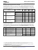
PACKAGE MATERIALS INFORMATION www.ti.com 23-Sep-2013 TAPE AND REEL INFORMATION *All dimensions are nominal Device Package Package Pins Type Drawing ADC12130CIWMX/NOPB SOIC ADC12138CIMSAX/NOPB ADC12138CIWMX/NOPB SPQ Reel Reel A0 Diameter Width (mm) (mm) W1 (mm) B0 (mm) K0 (mm) P1 (mm) W Pin1 (mm) Quadrant 10.9 10.7 3.2 12.0 16.0 Q1 DW 16 1000 330.0 16.4 SSOP DB 28 2000 330.0 16.4 8.4 10.7 2.4 12.0 16.0 Q1 SOIC DW 28 1000 330.0 24.4 10.8 18.4 3.2 12.0 24.
PACKAGE MATERIALS INFORMATION www.ti.com 23-Sep-2013 *All dimensions are nominal Device Package Type Package Drawing Pins SPQ Length (mm) Width (mm) Height (mm) ADC12130CIWMX/NOPB SOIC DW 16 1000 367.0 367.0 38.0 ADC12138CIMSAX/NOPB SSOP DB 28 2000 367.0 367.0 38.0 ADC12138CIWMX/NOPB SOIC DW 28 1000 367.0 367.0 45.
MECHANICAL DATA MSSO002E – JANUARY 1995 – REVISED DECEMBER 2001 DB (R-PDSO-G**) PLASTIC SMALL-OUTLINE 28 PINS SHOWN 0,38 0,22 0,65 28 0,15 M 15 0,25 0,09 8,20 7,40 5,60 5,00 Gage Plane 1 14 0,25 A 0°–ā8° 0,95 0,55 Seating Plane 2,00 MAX 0,10 0,05 MIN PINS ** 14 16 20 24 28 30 38 A MAX 6,50 6,50 7,50 8,50 10,50 10,50 12,90 A MIN 5,90 5,90 6,90 7,90 9,90 9,90 12,30 DIM 4040065 /E 12/01 NOTES: A. B. C. D. All linear dimensions are in millimeters.
IMPORTANT NOTICE Texas Instruments Incorporated and its subsidiaries (TI) reserve the right to make corrections, enhancements, improvements and other changes to its semiconductor products and services per JESD46, latest issue, and to discontinue any product or service per JESD48, latest issue. Buyers should obtain the latest relevant information before placing orders and should verify that such information is current and complete.