
Datasheet
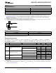


ADC121C021, ADC121C021Q, ADC121C027
www.ti.com
SNAS415F –JANUARY 2008–REVISED MARCH 2013
ADC121C021/ADC121C021Q/ADC121C027 I
2
C-Compatible, 12-Bit Analog-to-Digital
Converter with Alert Function
Check for Samples: ADC121C021, ADC121C021Q, ADC121C027
1
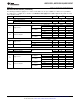
FEATURES
DESCRIPTION
These converters are low-power, monolithic, 12-bit,
23
• I
2
C-Compatible 2-Wire Interface Which
analog-to-digital converters (ADCs) that operates
Supports Standard (100kHz), Fast (400kHz),
from a +2.7 to 5.5V supply. The converter is based
and High Speed (3.4MHz) Modes
upon a successive approximation register
• Extended Power Supply Range (+2.7V to
architecture with an internal track-and-hold circuit that
+5.5V)
can handle input frequencies up to 11MHz. These
converters operate from a single supply which also
• Up to Nine Pin-Selectable Chip Addresses
serves as the reference. The device features an I
2
C-
(VSSOP Only)
compatible serial interface that operates in all three
• Out-of-Range Alert Function
speed modes, including high speed mode (3.4MHz).
• Automatic Power-Down Mode while Not
The ADC121C021's Alert feature provides an
Converting
interrupt that is activated when the analog input
• Very Small 6-Pin SOT and 8-Pin VSSOP
violates a programmable upper or lower limit value.
Packages
The device features an automatic conversion mode,
which frees up the controller and I
2
C interface. In this
• ADC121C021Q is an Automotive Grade
mode, the ADC continuously monitors the analog
Product that is AEC-Q100 Grade 2 Qualified
input for an "out-of-range" condition and provides an
interrupt if the measured voltage goes out-of-range.
APPLICATIONS
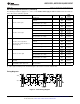
The ADC121C021 comes in two packages: a small 6-
• System Monitoring
pin SOT package with an alert output, and an 8-pin
• Peak Detection
VSSOP package with an alert output and two
• Portable Instruments
address selection inputs. The ADC121C021Q is
available in a 6-pin SOT package. The ADC121C027
• Medical Instruments
comes in a small 6-pin SOT package with an address
• Test Equipment
selection input. The ADC121C027 provides three pin-
• Automotive
selectable addresses while the 8-pin VSSOP version
of the ADC121C021 provides nine pin-selectable
addresses. Pin-compatible alternatives to the 6-pin
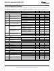
KEY SPECIFICATIONS
SOT options are available with additional address
• Resolution: 12 Bits (No Missing Codes)
options.
• Conversion Time: 1µs (Typ)
Normal power consumption using a +3V or +5V
• INL & DNL: ±1 LSB (Max) (Up to 22ksps)
supply is 0.26mW or 0.78mW, respectively. The
• Throughput Rate: 188.9 ksps (Max)
automatic power-down feature reduces the power
consumption to less than 1µW while not converting.
• Power Consumption (at 22 ksps)
Operation over the industrial temperature range of
– 3V Supply: 0.26 mW (Typ)
−40°C to +105°C is ensured. Their low power
– 5v Supply: 0.78 mW (Typ)
consumption and small packages make this family of
ADCs an excellent choice for use in battery operated
equipment.
The ADC121C021 and ADC121C027 are part of a
family of pin-compatible ADCs that also provide 8 and
10 bit resolution. For 8-bit ADCs see the
ADC081C021 and ADC081C027. For 10-bit ADCs
see the ADC101C021 and ADC101C027.
1
Please be aware that an important notice concerning availability, standard warranty, and use in critical applications of
Texas Instruments semiconductor products and disclaimers thereto appears at the end of this data sheet.
2I
2
C is a registered trademark of Phillips Corporation..
3All other trademarks are the property of their respective owners.
PRODUCTION DATA information is current as of publication date.
Copyright © 2008–2013, Texas Instruments Incorporated
Products conform to specifications per the terms of the Texas
Instruments standard warranty. Production processing does not
necessarily include testing of all parameters.