
Datasheet
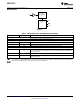
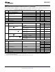


T/H
12-BIT
SUCCESSIVE
APPROXIMATION
ADC
SCLK
CS
SDATA
CONTROL
LOGIC
V
IN
ADC121S051
SNAS302H –JULY 2005–REVISED MARCH 2013
www.ti.com
Block Diagram
Figure 2.
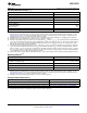
Table 1. PIN DESCRIPTIONS AND EQUIVALENT CIRCUITS
Pin No. Symbol Description
ANALOG I/O
3 V
IN
Analog input. This signal can range from 0V to V
A
DIGITAL I/O
4 SCLK Digital clock input. This clock directly controls the conversion and readout processes.
5 SDATA Digital data output. This clock directly controls the conversion and readout processes.
6 CS Chip select. On the falling edge of CS, a conversion process begins.
POWER SUPPLY
Positive supply pin. This pin should be connected to a quiet +2.7V to +5.25V source and
1 V
A
bypassed to GND with a 1 μF capacitor and a 0.1 μF monolithic capacitor located within 1
cm of the power pin.
2 GND The ground return for the supply and signals.
For package suffix CISD(X) only, it is recommended that the center pad should be
PAD GND
connected to ground.
These devices have limited built-in ESD protection. The leads should be shorted together or the device placed in conductive foam
during storage or handling to prevent electrostatic damage to the MOS gates.
2 Submit Documentation Feedback Copyright © 2005–2013, Texas Instruments Incorporated
Product Folder Links: ADC121S051