
Datasheet

1
2
3
4
5
6
7
8 9
10
11
12
13
14
15
16
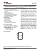
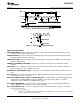
CS SCLK
V
A
DOUT
AGND DIN
IN0 V
D
IN1 DGND
IN2 IN7
IN3 IN6
IN4 IN5
ADC128S052
ADC128S052
www.ti.com
SNAS333D –AUGUST 2005–REVISED MARCH 2013
ADC128S052/ADC128S052Q 8-Channel, 200 kSPS to 500 kSPS, 12-Bit A/D Converter
Check for Samples: ADC128S052
1
FEATURES
DESCRIPTION
The ADC128S052 is a low-power, eight-channel
2
• ADC128S052Q is AECQ100 Qualified to
CMOS 12-bit analog-to-digital converter specified for
Grade1 and is Manufactured on an Automotive
conversion throughput rates of 200 kSPS to 500
Grade Flow
kSPS. The converter is based on a successive-
• Eight Input Channels
approximation register architecture with an internal
track-and-hold circuit. It can be configured to accept
• Variable Power Management
up to eight input signals at inputs IN0 through IN7.
• Independent Analog and Digital Supplies
The output serial data is straight binary and is
• SPI/QSPI/MICROWIRE/DSP Compatible
compatible with several standards, such as SPI,
• Packaged in 16-Lead TSSOP
QSPI, MICROWIRE, and many common DSP serial
interfaces.
APPLICATIONS
The ADC128S052 may be operated with independent
• Automotive Navigation
analog and digital supplies. The analog supply (V
A
)
• Portable Systems
can range from +2.7V to +5.25V, and the digital
supply (V
D
) can range from +2.7V to V
A
. Normal
• Medical Instruments
power consumption using a +3V or +5V supply is 1.6
• Mobile Communications
mW and 8.7 mW, respectively. The power-down
• Instrumentation and Control Systems
feature reduces the power consumption to 0.06 µW
using a +3V supply and 0.25 µW using a +5V supply.
KEY SPECIFICATIONS
The ADC128S052/ADC128S052Q is packaged in a
• Conversion Rate 200 kSPS to 500 kSPS
16-lead TSSOP package. The ADC128S052 is
guaranteed over the extended industrial
• DNL (VA = VD = 5.0 V) +1.3 / −0.9 LSB (max)
temperature range of −40°C to +105°C while the
• INL (VA = VD = 5.0 V) ±1.0 LSB (max)
ADC128S052Q is guaranteed to an AECQ100
• Power Consumption
Grade 1 automotive temperature range of −40°C
to +125°C.
– 3V Supply 1.6 mW (typ)
– 5V Supply 8.7 mW (typ)
Connection Diagram
1
Please be aware that an important notice concerning availability, standard warranty, and use in critical applications of
Texas Instruments semiconductor products and disclaimers thereto appears at the end of this data sheet.
2All trademarks are the property of their respective owners.
PRODUCTION DATA information is current as of publication date.
Copyright © 2005–2013, Texas Instruments Incorporated
Products conform to specifications per the terms of the Texas
Instruments standard warranty. Production processing does not
necessarily include testing of all parameters.