
Datasheet
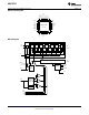
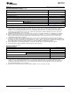
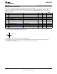

V
A
AGND
To Internal Circuitry
I/O
ADC12C105
SNAS417B –MAY 2007–REVISED AUGUST 2007
www.ti.com
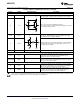
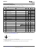
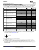
Dynamic Converter Electrical Characteristics at 95MSPS
Unless otherwise specified, the following specifications apply: AGND = DRGND = 0V, V
A
= +3.3V, V
DR
= +2.5V, Internal V
REF
= +1.2V, f
CLK
= 95 MHz, 50% Duty Cycle, DCS disabled, V
CM
= V
CMO
, C
L
= 5 pF/pin, . Typical values are for T
A
= 25°C.
Boldface limits apply for T
MIN
≤ T
A
≤ T
MAX
. All other limits apply for T
A
= 25°C
(1) (2)
Typical Units
Symbol Parameter Conditions Limits
(3)
(Limits)
(4)
DYNAMIC CONVERTER CHARACTERISTICS, A
IN
= -1dBFS
f
IN
= 10 MHz 71 dBFS
SNR Signal-to-Noise Ratio f
IN
= 70 MHz 70.5 dBFS
f
IN
= 240 MHz 69 dBFS
f
IN
= 10 MHz 90 dBFS
SFDR Spurious Free Dynamic Range f
IN
= 70 MHz 86 dBFS
f
IN
= 240 MHz 82 dBFS
f
IN
= 10 MHz 11.5 Bits
ENOB Effective Number of Bits f
IN
= 70 MHz 11.4 Bits
f
IN
= 240 MHz 11.1 Bits
f
IN
= 10 MHz −88 dBFS
THD Total Harmonic Disortion f
IN
= 70 MHz −85 dBFS
f
IN
= 240 MHz −80 dBFS
f
IN
= 10 MHz -95 dBFS
H2 Second Harmonic Distortion f
IN
= 70 MHz −90 dBFS
f
IN
= 240 MHz −85 dBFS
f
IN
= 10 MHz −90 dBFS
H3 Third Harmonic Distortion f
IN
= 70 MHz −86 dBFS
f
IN
= 240 MHz −82 dBFS
f
IN
= 10 MHz 70.9 dBFS
SINAD Signal-to-Noise and Distortion Ratio f
IN
= 70 MHz 70.35 dBFS
f
IN
= 240 MHz 68.7 dBFS
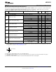
POWER SUPPLY CHARACTERISTICS
I
A
Analog Supply Current Full Operation 115 mA (max)
I
DR
Digital Output Supply Current Full Operation
(5)
14.5 mA
Power Consumption Excludes I
DR
(5)
380 mW (max)
(1) The inputs are protected as shown below. Input voltage magnitudes above V
A
or below GND will not damage this device, provided
current is limited per Absolute Maximum Ratings, Note 4. However, errors in the A/D conversion can occur if the input goes above 2.6V
or below GND as described in the Operating Ratings section.
(2) With a full scale differential input of 2V
P-P
, the 12-bit LSB is 488 µV.
(3) Typical figures are at T
A
= 25°C and represent most likely parametric norms at the time of product characterization. The typical
specifications are not ensured.
(4) Parameters specified in dBFS indicate the value that would be attained with a full-scale input signal.
(5) I
DR
is the current consumed by the switching of the output drivers and is primarily determined by load capacitance on the output pins,
the supply voltage, V
DR
, and the rate at which the outputs are switching (which is signal dependent). I
DR
=V
DR
(C
0
x f
0
+ C
1
x f
1
+....C
11
x
f
11
) where V
DR
is the output driver power supply voltage, C
n
is total capacitance on the output pin, and f
n
is the average frequency at
which that pin is toggling.
10 Submit Documentation Feedback Copyright © 2007, Texas Instruments Incorporated
Product Folder Links: ADC12C105