
Datasheet

ADC12C105
SNAS417B –MAY 2007–REVISED AUGUST 2007
www.ti.com
Typical Performance Characteristics (continued)
Unless otherwise specified, the following specifications apply: AGND = DRGND = 0V, V
A
= +3.3V, V
DR
= +2.5V, Internal V
REF
= +1.2V, f
CLK
= 105 MHz, 50% Duty Cycle, DCS disabled, V
CM
= V
CMO
, f
IN
= 10 MHz, C
L
= 5 pF/pin. Typical values are for T
A
= 25°C.
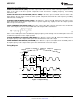
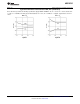
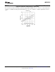
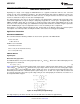
SNR, SINAD, SFDR vs. Temperature Distortion vs. Temperature
Figure 23. Figure 24.
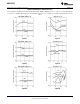
Spectral Response @ 10 MHz Input Spectral Response @ 70 MHz Input
Figure 25. Figure 26.
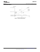
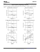
Spectral Response @ 240 MHz Input Intermodulation Distortion, f
IN
1= 19.5 MHz, f
IN
2 = 20.5 MHz
Figure 27. Figure 28.
18 Submit Documentation Feedback Copyright © 2007, Texas Instruments Incorporated
Product Folder Links: ADC12C105