
Datasheet

ADC12C105
SNAS417B –MAY 2007–REVISED AUGUST 2007
www.ti.com
FUNCTIONAL DESCRIPTION
Operating on a single +3.3V supply, the ADC12C105 uses a pipeline architecture and has error correction
circuitry to help ensure maximum performance. The differential analog input signal is digitized to 12 bits. The
user has the choice of using an internal 1.2V stable reference, or using an external 1.2V reference. Any external
reference is buffered on-chip to ease the task of driving that pin.
The output word rate is the same as the clock frequency. The analog input is acquired at the rising edge of the
clock and the digital data for a given sample is delayed by the pipeline for 7 clock cycles. The digital outputs are
CMOS compatible signals that are clocked by a synchronous data ready output signal (DRDY, pin 21) at the
same rate as the clock input. Duty cycle stabilization and output data format are selectable using the quad state
function OF/DCS pin (pin 12). The output data can be set for offset binary or two's complement.
Power-down is selectable using the PD pin (pin 30). A logic high on the PD pin reduces the converter power
consumption. For normal operation, the PD pin should be connected to the analog ground (AGND).
Applications Information
OPERATING CONDITIONS
We recommend that the following conditions be observed for operation of the ADC12C105:
2.7V ≤ V
A
≤ 3.6V
2.4V ≤ V
DR
≤ V
A
20 MHz ≤ f
CLK
≤ 105 MHz
1.2V internal reference
V
REF
= 1.2V (for an external reference)
V
CM
= 1.5V (from V
CMO
)
ANALOG INPUTS
Signal Inputs
Differential Analog Input Pins
The ADC12C105 has one pair of analog signal input pins, V
IN
+ and V
IN
−, which form a differential input pair. The
input signal, V
IN
, is defined as
V
IN
= (V
IN
+) – (V
IN
−) (4)
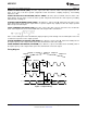
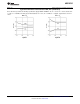
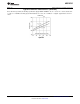
Figure 30 shows the expected input signal range. Note that the common mode input voltage, V
CM
, should be
1.5V. Using V
CMO
(pin 32) for V
CM
will ensure the proper input common mode level for the analog input signal.
The positive peaks of the individual input signals should each never exceed 2.6V. Each analog input pin of the
differential pair should have a maximum peak-to-peak voltage of 1V, be 180° out of phase with each other and
be centered around V
CM
.The peak-to-peak voltage swing at each analog input pin should not exceed the 1V or
the output data will be clipped.
Figure 30. Expected Input Signal Range
For single frequency sine waves the full scale error in LSB can be described as approximately
20 Submit Documentation Feedback Copyright © 2007, Texas Instruments Incorporated
Product Folder Links: ADC12C105