
Datasheet


ADC12C105
SNAS417B –MAY 2007–REVISED AUGUST 2007
www.ti.com
One short-coming of using a transformer to achieve the single-ended to differential conversion is that most RF
transformers have poor low frequency performance. A differential amplifier can be used to drive the analog inputs
for low frequency applications. The amplifier must be fast enough to settle from the charging glitches on the
analog input resulting from the sample-and-hold operation before the clock goes high and the sample is passed
to the ADC core.
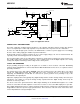
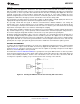
The SFDR performance of the converter depends on the external signal conditioning circuity used, as this affects
how quickly the sample-and-hold charging glitch will settle. An external resistor and capacitor network as shown
in Figure 34 should be used to isolate the charging glitches at the ADC input from the external driving circuit and
to filter the wideband noise at the converter input. These components should be placed close to the ADC inputs
because the analog input of the ADC is the most sensitive part of the system, and this is the last opportunity to
filter that input. For Nyquist applications the RC pole should be at the ADC sample rate. The ADC input
capacitance in the sample mode should be considered when setting the RC pole. For wideband undersampling
applications, the RC pole should be set at least 1.5 to 2 times the maximum input frequency to maintain a linear
delay response.
Input Common Mode Voltage
The input common mode voltage, V
CM
, should be in the range of 1.4V to 1.6V and be a value such that the peak
excursions of the analog signal do not go more negative than ground or more positive than 2.6V. It is
recommended to use V
CMO
(pin 32) as the input common mode voltage.
If the ADC12C105 is operated with V
A
=3.6V, a resistor of approximately 1KΩ should be used from the V
CMO
pin
to AGND.This will help maintain stability over the entire temperature range when using a high supply voltage.
Reference Pins
The ADC12C105 is designed to operate with an internal or external 1.2V reference. The internal 1.2 Volt
reference is the default condition when no external reference input is applied to the V
REF
pin. If a voltage is
applied to the V
REF
pin, then that voltage is used for the reference. The V
REF
pin should always be bypassed to
ground with a 0.1 µF capacitor close to the reference input pin.
It is important that all grounds associated with the reference voltage and the analog input signal make connection
to the ground plane at a single, quiet point to minimize the effects of noise currents in the ground path.
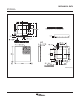
The Reference Bypass Pins (V
RP
, V
CMO
, and V
RN
) are made available for bypass purposes. These pins should
each be bypassed to AGND with a low ESL (equivalent series inductance) 1 µF capacitor placed very close to
the pin to minimize stray inductance. A 0.1 µF capacitor should be placed between V
RP
and V
RN
as close to the
pins as possible, and a 1 µF capacitor should be placed in parallel. This configuration is shown in Figure 34. It is
necessary to avoid reference oscillation, which could result in reduced SFDR and/or SNR. V
CMO
may be loaded
to 1mA for use as a temperature stable 1.5V reference. The remaining pins should not be loaded.
Smaller capacitor values than those specified will allow faster recovery from the power down mode, but may
result in degraded noise performance. Loading any of these pins, other than V
CMO
may result in performance
degradation.
The nominal voltages for the reference bypass pins are as follows:
V
CMO
= 1.5 V
V
RP
= 2.0 V
V
RN
= 1.0 V
OF/DCS Pin
Duty cycle stabilization and output data format are selectable using this quad state function pin. When enabled,
duty cycle stabilization can compensate for clock inputs with duty cycles ranging from 30% to 70% and generate
a stable internal clock, improving the performance of the part. With OF/DCS = V
A
the output data format is 2's
complement and duty cycle stabilization is not used. With OF/DCS = AGND the output data format is offset
binary and duty cycle stabilization is not used. With OF/DCS = (2/3)*V
A
the output data format is 2's complement
and duty cycle stabilization is applied to the clock. If OF/DCS is (1/3)*V
A
the output data format is offset binary
and duty cycle stabilization is applied to the clock. While the sense of this pin may be changed "on the fly," doing
this is not recommended as the output data could be erroneous for a few clock cycles after this change is made.
22 Submit Documentation Feedback Copyright © 2007, Texas Instruments Incorporated
Product Folder Links: ADC12C105