
Datasheet


AGND
AGND
ADC12C105
V
A
V
A
V
DR
3
8
20
CHOKE
0.1 PF
D7
D6
D5
D4
(MSB) D11
D10
D9
D8
D3
D2
D1
(LSB) D0
2 x 0.1 PF
31
V
REF
+
10 PF
+3.3V
50
32
2
1
V
CMO
V
RP
V
RN
T1
ADT1-1WT
0.1 PF
20
20
0.1 PF
1
2
V
IN
+
V
IN
-
OF/DCC
CLK
Clock In
OF/DCS
PD
PD
0.1 PF1 PF
0.1 PF
15
16
17
18
19
23
24
25
26
27
28
29
2.4 to V
A
Volts
4
7
22
DRGND
5
6
30
12
11
V
IN
74LVTH162374
Output
Word
CLK
10 PF
18 pF
10
V
A
DRDY
21
9
0.1 PF
1 PF
0.1 PF
0.1 PF
0.1 PF
ADC12C105
SNAS417B –MAY 2007–REVISED AUGUST 2007
www.ti.com
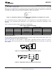
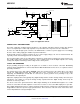
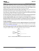
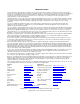
Figure 34. Application Circuit
POWER SUPPLY CONSIDERATIONS
The power supply pins should be bypassed with a 0.1 µF capacitor and with a 100 pF ceramic chip capacitor
close to each power pin. Leadless chip capacitors are preferred because they have low series inductance.
As is the case with all high-speed converters, the ADC12C105 is sensitive to power supply noise. Accordingly,
the noise on the analog supply pin should be kept below 100 mV
P-P
.
No pin should ever have a voltage on it that is in excess of the supply voltages, not even on a transient basis. Be
especially careful of this during power turn on and turn off.
The V
DR
pin provides power for the output drivers and may be operated from a supply in the range of 2.4V to V
A
.
This enables lower power operation, reduces the noise coupling effects from the digital outputs to the analog
circuitry and simplifies interfacing to lower voltage devices and systems.
LAYOUT AND GROUNDING
Proper grounding and proper routing of all signals are essential to ensure accurate conversion. Maintaining
separate analog and digital areas of the board, with the ADC12C105 between these areas, is required to achieve
specified performance.
The ground return for the data outputs (DRGND) carries the ground current for the output drivers. The output
current can exhibit high transients that could add noise to the conversion process. To prevent this from
happening, the DRGND pins should NOT be connected to system ground in close proximity to any of the
ADC12C105's other ground pins.
Capacitive coupling between the typically noisy digital circuitry and the sensitive analog circuitry can lead to poor
performance. The solution is to keep the analog circuitry separated from the digital circuitry, and to keep the
clock line as short as possible.
The effects of the noise generated from the ADC output switching can be minimized through the use of 22Ω
resistors in series with each data output line. Locate these resistors as close to the ADC output pins as possible.
Since digital switching transients are composed largely of high frequency components, total ground plane copper
weight will have little effect upon the logic-generated noise. This is because of the skin effect. Total surface area
is more important than is total ground plane area.
24 Submit Documentation Feedback Copyright © 2007, Texas Instruments Incorporated
Product Folder Links: ADC12C105