
Datasheet
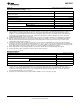
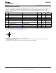

DRGND
V
DR
DGND
V
A
AGND
V
A
ADC12C105
SNAS417B –MAY 2007–REVISED AUGUST 2007
www.ti.com
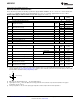
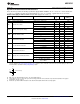
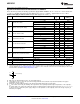
Pin Descriptions and Equivalent Circuits (continued)
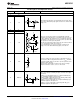
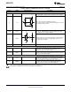
Pin No. Symbol Equivalent Circuit Description
DIGITAL I/O
The clock input pin.
11 CLK
The analog input is sampled on the rising edge of the clock input.
This is a two-state input controlling Power Down.
30 PD PD = V
A
, Power Down is enabled and power dissipation is reduced.
PD = AGND, Normal operation.
Digital data output pins that make up the 12-bit conversion result. D0
15-19,
D0–D11 (pin 15) is the LSB, while D11 (pin 29) is the MSB of the output
23-29
word. Output levels are CMOS compatible.
Data Ready Strobe. The data output transition is synchronized with
21 DRDY the falling edge of this signal. This signal switches at the same
frequency as the CLK input.
13, 14 NC No internal connection
ANALOG POWER
Positive analog supply pins. These pins should be connected to a
3, 8, 10 V
A
quiet voltage source and be bypassed to AGND with 0.1 µF
capacitors located close to the power pins.
The ground return for the analog supply.
4, 7, 9,
AGND The exposed pad on back of package must be soldered to ground
Exposed Pad
plane to ensure rated performance.
DIGITAL POWER
Positive driver supply pin for the output drivers. This pin should be
20 V
DR
connected to a quiet voltage source and be bypassed to DRGND
with a 0.1 µF capacitor located close to the power pin.
The ground return for the digital output driver supply. This pins
22 DRGND should be connected to the system digital ground, but not be
connected in close proximity to the ADC's AGND pins.
These devices have limited built-in ESD protection. The leads should be shorted together or the device placed in conductive foam
during storage or handling to prevent electrostatic damage to the MOS gates.
4 Submit Documentation Feedback Copyright © 2007, Texas Instruments Incorporated
Product Folder Links: ADC12C105