
Datasheet

V
A
AGND
To Internal Circuitry
I/O
ADC12C105
SNAS417B –MAY 2007–REVISED AUGUST 2007
www.ti.com
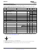
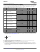
Logic and Power Supply Electrical Characteristics
Unless otherwise specified, the following specifications apply: AGND = DRGND = 0V, V
A
= +3.3V, V
DR
= +2.5V, Internal V
REF
= +1.2V, f
CLK
= 105 MHz, 50% Duty Cycle, DCS disabled, V
CM
= V
CMO
, C
L
= 5 pF/pin. Typical values are for T
A
= 25°C.
Boldface limits apply for T
MIN
≤ T
A
≤ T
MAX
. All other limits apply for T
A
= 25°C
(1) (2)
Units
Symbol Parameter Conditions Typical
(3)
Limits
(Limits)
DIGITAL INPUT CHARACTERISTICS (CLK, PD)
V
IN(1)
Logical “1” Input Voltage V
D
= 3.6V 2.0 V (min)
V
IN(0)
Logical “0” Input Voltage V
D
= 3.0V 0.8 V (max)
I
IN(1)
Logical “1” Input Current V
IN
= 3.3V 10 µA
I
IN(0)
Logical “0” Input Current V
IN
= 0V −10 µA
C
IN
Digital Input Capacitance 5 pF
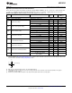
DIGITAL OUTPUT CHARACTERISTICS (D0–D13, DRDY)
V
OUT(1)
Logical “1” Output Voltage I
OUT
= −0.5 mA , V
DR
= 2.4V 2.0 V (min)
V
OUT(0)
Logical “0” Output Voltage I
OUT
= 1.6 mA, V
DR
= 2.4V 0.4 V (max)
+I
SC
Output Short Circuit Source Current V
OUT
= 0V −10 mA
−I
SC
Output Short Circuit Sink Current V
OUT
= V
DR
10 mA
C
OUT
Digital Output Capacitance 5 pF
POWER SUPPLY CHARACTERISTICS
I
A
Analog Supply Current Full Operation 121 141 mA (max)
I
DR
Digital Output Supply Current Full Operation
(4)
16 mA
Power Consumption Excludes I
DR
(4)
400 466 mW (max)
Power Down Power Consumption Clock disabled 7.5 mW
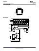
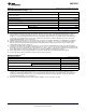
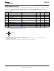
(1) The inputs are protected as shown below. Input voltage magnitudes above V
A
or below GND will not damage this device, provided
current is limited per Absolute Maximum Ratings, Note 4. However, errors in the A/D conversion can occur if the input goes above 2.6V
or below GND as described in the Operating Ratings section.
(2) With a full scale differential input of 2V
P-P
, the 12-bit LSB is 488 µV.
(3) Typical figures are at T
A
= 25°C and represent most likely parametric norms at the time of product characterization. The typical
specifications are not ensured.
(4) I
DR
is the current consumed by the switching of the output drivers and is primarily determined by load capacitance on the output pins,
the supply voltage, V
DR
, and the rate at which the outputs are switching (which is signal dependent). I
DR
=V
DR
(C
0
x f
0
+ C
1
x f
1
+....C
11
x
f
11
) where V
DR
is the output driver power supply voltage, C
n
is total capacitance on the output pin, and f
n
is the average frequency at
which that pin is toggling.
8 Submit Documentation Feedback Copyright © 2007, Texas Instruments Incorporated
Product Folder Links: ADC12C105