
Datasheet
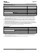
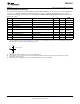

V
A
AGND
To Internal Circuitry
I/O
ADC12C105
www.ti.com
SNAS417B –MAY 2007–REVISED AUGUST 2007
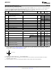
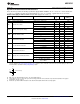
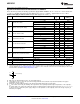
Timing and AC Characteristics
Unless otherwise specified, the following specifications apply: AGND = DRGND = 0V, V
A
= +3.3V, V
DR
= +2.5V, Internal V
REF
= +1.2V, f
CLK
= 105 MHz, 50% Duty Cycle, DCS disabled, V
CM
= V
CMO
, C
L
= 5 pF/pin. Typical values are for T
A
= 25°C.
Timing measurements are taken at 50% of the signal amplitude. Boldface limits apply for T
MIN
≤ T
A
≤ T
MAX
. All other limits
apply for T
A
= 25°C
(1) (2)
Units
Symb Parameter Conditions Typical
(3)
Limits
(Limits)
Maximum Clock Frequency 105 MHz (max)
Minimum Clock Frequency 20 MHz (min)
t
CH
Clock High Time 4 ns
t
CL
Clock Low Time 4 ns
t
CONV
Conversion Latency 7 Clock Cycles
3 ns (min)
t
OD
Output Delay of CLK to DATA Relative to rising edge of CLK
(4)
5.76
7.3 ns (max)
t
SU
Data Output Setup Time Relative to DRDY 4.5 3.7 ns (min)
t
H
Data Output Hold Time Relative to DRDY 4.5 3.8 ns (min)
t
AD
Aperture Delay 0.6 ns
t
AJ
Aperture Jitter 0.1 ps rms
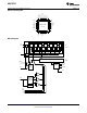
(1) The inputs are protected as shown below. Input voltage magnitudes above V
A
or below GND will not damage this device, provided
current is limited per Absolute Maximum Ratings, Note 4. However, errors in the A/D conversion can occur if the input goes above 2.6V
or below GND as described in the Operating Ratings section.
(2) With a full scale differential input of 2V
P-P
, the 12-bit LSB is 488 µV.
(3) Typical figures are at T
A
= 25°C and represent most likely parametric norms at the time of product characterization. The typical
specifications are not ensured.
(4) This parameter is specified by design and/or characterization and is not tested in production.
Copyright © 2007, Texas Instruments Incorporated Submit Documentation Feedback 9
Product Folder Links: ADC12C105