
Datasheet

ADC12DC105
www.ti.com
SNAS469A –SEPTEMBER 2008–REVISED OCTOBER 2008
ADC12DC105 Dual 12-Bit, 105 MSPS A/D Converter with CMOS Outputs
Check for Samples: ADC12DC105
1
FEATURES
DESCRIPTION
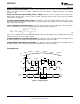
The ADC12DC105 is a high-performance CMOS
2
• Internal Sample-and-Hold Circuit and Precision
analog-to-digital converter capable of converting two
Reference
analog input signals into 12-bit digital words at rates
• Low Power Consumption
up to 105 Mega Samples Per Second (MSPS). These
• Clock Duty Cycle Stabilizer
converters use a differential, pipelined architecture
with digital error correction and an on-chip sample-
• Single +3.0V or +3.3V Supply Operation
and-hold circuit to minimize power consumption and
• Power-Down Mode
the external component count, while providing
• Offset Binary or 2's Complement Output Data
excellent dynamic performance. A unique sample-
Format
and-hold stage yields a full-power bandwidth of 1
GHz. The ADC12DC080/105 may be operated from a
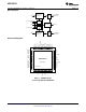
• 60-Pin WQFN Package, (9x9x0.8mm, 0.5mm
single +3.0V or +3.3V power supply. A power-down
Pin-Pitch)
feature reduces the power consumption to very low
levels while still allowing fast wake-up time to full
APPLICATIONS
operation. The differential inputs provide a 2V full
scale differential input swing. A stable 1.2V internal
• High IF Sampling Receivers
voltage reference is provided, or the ADC12DC105
• Wireless Base Station Receivers
can be operated with an external 1.2V reference.
• Test and Measurement Equipment
Output data format (offset binary versus 2's
• Communications Instrumentation
complement) and duty cycle stabilizer are pin-
selectable. The duty cycle stabilizer maintains
• Portable Instrumentation
performance over a wide range of clock duty cycles.
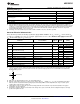
KEY SPECIFICATIONS
The ADC12DC105 is available in a 60-lead WQFN
package and operates over the industrial temperature
• Resolution: 12 Bits
range of −40°C to +85°C.
• Conversion Rate: 105 MSPS
• SNR (f
IN
= 170 MHz): 69 dBFS (Typ)
• SFDR (f
IN
= 170 MHz): 83 dBFS (Typ)
• Full Power Bandwidth: 1 GHz (Typ)
• Power Consumption
– 690 mW (Typ), V
A
= 3.0V
– 800 mW (Typ), V
A
= 3.3V
1
Please be aware that an important notice concerning availability, standard warranty, and use in critical applications of
Texas Instruments semiconductor products and disclaimers thereto appears at the end of this data sheet.
2All trademarks are the property of their respective owners.
PRODUCTION DATA information is current as of publication date.
Copyright © 2008, Texas Instruments Incorporated
Products conform to specifications per the terms of the Texas
Instruments standard warranty. Production processing does not
necessarily include testing of all parameters.