
Datasheet
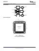

DRGND
V
DR
V
A
DRGND
ADC12DC105
SNAS469A –SEPTEMBER 2008–REVISED OCTOBER 2008
www.ti.com
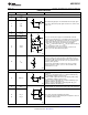
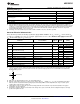
PIN DESCRIPTIONS (continued)
Pin No. Symbol Equivalent Circuit Description
Digital data output pins that make up the 12-bit conversion result for
42-49, DA0-DA7,
Channel A. DA0 (pin 42) is the LSB, while DA11 (pin 55) is the MSB
52-55 DA8-DA11
of the output word. Output levels are CMOS compatible.
Digital data output pins that make up the 12-bit conversion result for
23-24, DB0-DB1,
Channel B. DB0 (pin 23) is the LSB, while DB11 (pin 36) is the MSB
27-36 DB3-DB11
of the output word. Output levels are CMOS compatible.
Data Ready Strobe. The data output transition is synchronized with
39 DRDY the falling edge of this signal. This signal switches at the same
frequency as the CLK input.
(6)
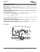
ANALOG POWER
Positive analog supply pins. These pins should be connected to a
8, 16, 17, 58,
V
A
quiet source and be bypassed to AGND with 0.1 µF capacitors
60
located close to the power pins.
The ground return for the analog supply.
1, 4, 12, 15,
AGND The exposed pad on back of package must be soldered to ground
Exposed Pad
plane to ensure rated performance.
DIGITAL POWER
Positive driver supply pin for the output drivers. This pin should be
26, 38,50 V
DR
connected to a quiet voltage source and be bypassed to DRGND
with a 0.1 µF capacitor located close to the power pin.
The ground return for the digital output driver supply. This pins
25, 37, 51 DRGND should be connected to the system digital ground, but not be
connected in close proximity to the ADC's AGND pins.
These devices have limited built-in ESD protection. The leads should be shorted together or the device placed in conductive foam
during storage or handling to prevent electrostatic damage to the MOS gates.
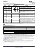
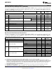
Absolute Maximum Ratings
(1)(2)(3)(4)(5)
Supply Voltage (V
A
, V
DR
) −0.3V to 4.2V
Voltage on Any Pin (Not to exceed 4.2V) −0.3V to (V
A
+0.3V)
Input Current at Any Pin other than Supply Pins
(6)
±5 mA
Package Input Current
(6)
±50 mA
Max Junction Temp (T
J
) +150°C
Thermal Resistance (θ
JA
) 30°C/W
Human Body Model
(7)
2500V
ESD Rating
Machine Model
(7)
250V
Storage Temperature −65°C to +150°C
(1) All voltages are measured with respect to GND = AGND = DRGND = 0V, unless otherwise specified.
(2) Absolute Maximum Ratings indicate limits beyond which damage to the device may occur. Operating Ratings indicate conditions for
which the device is guaranteed to be functional, but do not guarantee specific performance limits. For guaranteed specifications and test
conditions, see the Electrical Characteristics. The guaranteed specifications apply only for the test conditions listed. Some performance
characteristics may degrade when the device is not operated under the listed test conditions. Operation of the device beyond the
maximum Operating Ratings is not recommended.
(3) Soldering process must comply with National Semiconductor's Reflow Temperature Profile specifications. Refer to
www.ti.com/packaging.
(4) If Military/Aerospace specified devices are required, please contact the Texas Instruments Sales Office/Distributors for availability and
specifications.
(5) Reflow temperature profiles are different for lead-free and non-lead-free packages.
(6) When the input voltage at any pin exceeds the power supplies (that is, V
IN
< AGND, or V
IN
> V
A
), the current at that pin should be
limited to ±5 mA. The ±50 mA maximum package input current rating limits the number of pins that can safely exceed the power
supplies with an input current of ±5 mA to 10.
(7) Human Body Model is 100 pF discharged through a 1.5 kΩ resistor. Machine Model is 220 pF discharged through 0 Ω.
4 Submit Documentation Feedback Copyright © 2008, Texas Instruments Incorporated
Product Folder Links: ADC12DC105