
Datasheet

- 17 -
Copyright 2011 National Semiconductor Corporation
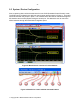
2.5.4 Right Panels - Registers
Next, configure the hardware (including the ADC) using the Registers control panel on the right
side. This is the most important of all the panels for controlling the ADC12D1X00RFRB.
This panel has twelve sub-tabs that control the settings of the board and registers inside the
ADC12D1X00RF. The twelve sub-tabs are shown below and include; Settings, Config, Cal
Adjust, I-channel, Q-channel, DES Adjust, t
AD
Adjust, AutoSync, and Temperature. The last
three tabs are register contents so that the user may verify register settings to be programmed
in the system.
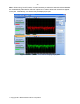
Figure 10: The top level of the Register panel showing the available tabs
The following is a short description of each tab under the Register panel.
Settings:
This tab gives choice of either External Clock or Internal Clock, and buttons to
initiate FPGA Reset, Reset Registers and Calibrate ADC. Calibration of the ADC should be
performed if changes occur such as device temperature, mode changes (single channel to dual
channel, single edge sampling (Non-DES) to double edge sampling (DES). For more
information, refer to the Calibration section of the ADC12D1X00RF datasheet. The H/W Trigger
function is also enabled using the check box on this tab.
Note: If the Internal Clock is selected, then the External Clock signal generator should be
disconnected or switched off to prevent performance degradation.